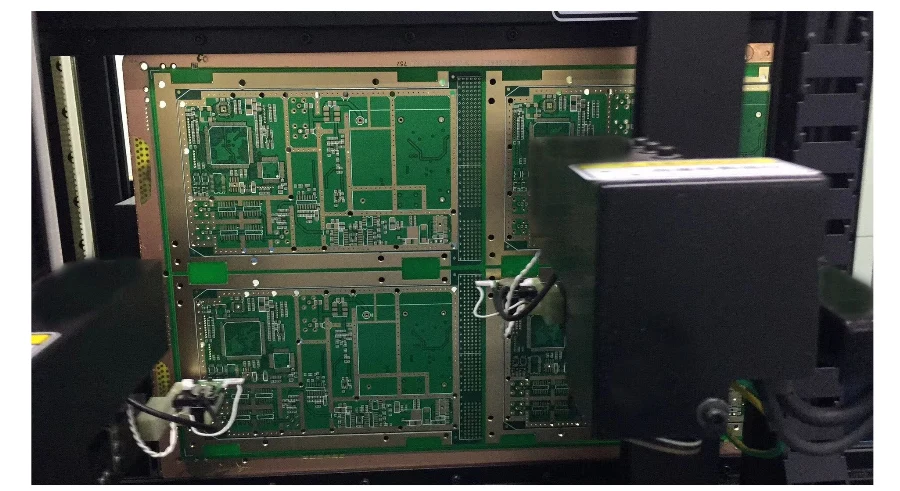
At Highleap PCB Factory, we specialize in designing and manufacturing high-quality RF PCBs. We know that in RF design, even small performance deviations can cause significant system failures. That's why we offer a full suite of testing services to ensure that your RF PCBs meet the highest standards of reliability and performance.
Our testing process goes beyond basic functionality. We conduct temperature cycling, humidity testing, vibration testing, and power cycling to test your boards under real-world conditions. We use advanced, specialized equipment to measure high-frequency signals accurately, ensuring your PCBs perform at their best, even in the most demanding environments.
Essential RF Test Equipment and Methods
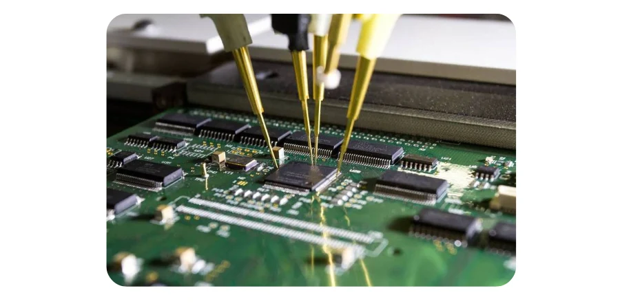
Modern RF testing centers around the Vector Network Analyzer (VNA), which measures how RF energy flows through your circuit. Think of it as a sophisticated RF multimeter that can characterize impedance, gain, loss, and phase relationships across frequency.
S-Parameter Measurements form the foundation of RF characterization:
- S11 (Return Loss): How much energy reflects back from the input
- S21 (Insertion Loss/Gain): How much energy passes through the circuit
- S12 (Reverse Isolation): Unwanted feedback from output to input
- S22 (Output Return Loss): Output impedance matching characteristics
Testing Frequency Ranges
Standard VNA Testing
Millimeter-Wave Extensions
Advanced mmWave Testing
Time Domain Reflectometry (TDR) provides a different perspective by sending fast pulses down transmission lines and analyzing reflections. TDR excels at locating impedance discontinuities and measuring trace characteristics. When you see an impedance bump on a TDR plot, you know exactly where on the PCB it occurs.
Spectrum analyzers complement VNA measurements by revealing signal purity. They show harmonic content, spurious emissions, and phase noise characteristics that determine real-world performance in communication systems.
Calibration and Measurement Accuracy
Accurate RF measurements depend entirely on proper calibration. At gigahertz frequencies, test cables, connectors, and probe tips all introduce measurement errors that must be removed through calibration.
The industry standard SOLT calibration (Short-Open-Load-Through) establishes reference planes at the measurement points. This process mathematically removes the effects of test equipment, leaving only the device-under-test characteristics.
Calibration Standards must be precisely characterized:
- Short Circuit: Known reflection with 180-degree phase shift
- Open Circuit: Known reflection with zero phase shift
- 50-Ohm Load: Known absorption with no reflection
- Through Connection: Known transmission with minimal loss
Environmental factors significantly impact measurement accuracy. Temperature changes affect cable length and connector dimensions. Humidity can alter dielectric properties. Vibration introduces phase noise. Professional RF testing requires environmental control and thermal stabilization.
Measurement uncertainty becomes critical when validating tight specifications. A ±0.1 dB measurement uncertainty means little when testing a 20 dB specification, but it's crucial when validating a 3 dB requirement.
Impedance Control Verification
TDR Impedance Profiling
Measures impedance variations along trace lengths to identify width or dielectric issues.
Manufacturing Test Coupons
Enable 100% impedance testing without damaging functional circuits on panels.
Network Analyzer Measurements
Validate frequency-dependent impedance behavior critical for high-frequency performance.
Statistical Process Control
Monitor impedance trends to identify and correct manufacturing variations in real-time.
Comprehensive impedance verification ensures signal integrity and prevents performance issues in high-frequency applications.
Environmental and Reliability Testing
RF circuits must perform reliably across varying environmental conditions, including wide temperature ranges, humidity fluctuations, and mechanical stress. Environmental testing is essential for validating design margins and identifying potential failure modes.
- Temperature Cycling: This test subjects circuits to repeated cycles of expansion and contraction, simulating extreme temperature changes. It helps identify weak solder joints, material compatibility issues, and temperature-dependent performance variations.
- Humidity Testing: Circuits are exposed to high moisture levels to assess how humidity impacts dielectric properties and can lead to corrosion. While RF circuits using PTFE materials generally show strong resistance, components such as solder masks and packaging materials may be more vulnerable.
- Vibration Testing: Mechanical robustness is critical for RF circuits in applications like automotive and aerospace. Vibration testing ensures that high-Q RF circuits remain stable and maintain frequency accuracy under mechanical stress, preventing resonance-related issues.
- Power Cycling: By stressing active components through thermal cycling under electrical load, this test accelerates failure mechanisms that might not be observed in standalone thermal or electrical stress testing, providing deeper insights into long-term reliability.
Ready to ensure your RF designs meet the highest performance and reliability standards? Our comprehensive environmental and reliability testing services give you the confidence to launch products that will perform under real-world conditions.
Testing Service Highlights
Fast Turnaround
- 24-48 hour test reports
- Rush testing available
- Real-time measurement updates
- Express prototype validation
Advanced Analysis
- Expert data interpretation
- Design optimization recommendations
- Root cause analysis
- Performance improvement strategies
Comprehensive Reports
- Detailed measurement data
- Graphical analysis
- Compliance verification
- Actionable recommendations
Cost Optimization in RF PCB Testing
Effective RF PCB testing not only ensures your designs meet performance requirements but also helps optimize development costs. By identifying potential issues early and performing targeted tests, we prevent costly redesigns and delays. Our efficient, comprehensive testing process maximizes product reliability while minimizing unnecessary testing, making it a cost-effective solution for both prototypes and large production runs.
Ready to ensure your RF designs meet the highest performance and reliability standards? Our comprehensive environmental and reliability testing services give you the confidence to launch products that will perform under real-world conditions.
🏆 Professional RF Testing Services
Comprehensive validation from prototype through production qualification
Schedule TestingRelated RF PCB Resources
Explore our comprehensive collection of RF PCB guides and services:
Design & Engineering
- RF PCB Design - Complete design principles and layout guidelines
- RF PCB Impedance Control - Precise impedance matching techniques
- High-Frequency Circuit Board - Advanced high-frequency design considerations
Manufacturing & Materials
- RF PCB Manufacturing - Professional manufacturing processes and capabilities
- RF PCB Materials - Material selection guide for optimal RF performance
- RF PCB Assembly - Expert assembly services and best practices
Specialized Applications
- Microwave PCB - Microwave frequency PCB design and testing solutions
💡 Need expert guidance on your RF PCB project? Our experienced team is ready to help you achieve optimal performance and reliability.