
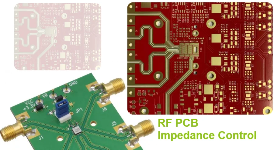
RF PCB impedance control is the coordinated design, fabrication and verification of transmission-line geometry so a finished interconnect meets its specified characteristic impedance. It is not the same as impedance matching at a component port, and a passing coupon does not by itself prove insertion loss, return loss or the complete RF channel.
Key Takeaways
- Define impedance by layer, structure, reference plane, target, tolerance and test method—not by adding “50 ohm” beside a net.
- Use the fabricator’s released stack-up and actual material data before finalizing trace width and gap.
- Model finished geometry, including etched sidewalls, copper thickness, solder mask and frequency-dependent material behavior where performance requires it.
- TDR coupons verify representative transmission-line cross-sections; VNA/S-parameter testing evaluates frequency-domain channel behavior.
- Set tolerance from system margin and manufacturing capability. No universal ±3%, ±5% or ±10% value fits every RF board.
Table of Contents
- What does controlled impedance prove?
- Which transmission-line structure should you use?
- How do design and fabrication stay correlated?
- TDR coupon vs board TDR vs VNA
- How should impedance acceptance be specified?
- Common impedance failures
- RF PCB impedance-control RFQ checklist
- Frequently asked questions
What Does Controlled Impedance Prove?
For a uniform transmission line, characteristic impedance can be expressed as Z₀ = √(L′/C′), where L′ and C′ are inductance and capacitance per unit length. Width, finished copper thickness, dielectric height, dielectric properties, adjacent copper and reference planes shape those values.
Mismatch occurs when a wave reaches a different impedance. The reflection coefficient Γ = (ZL − Z₀)/(ZL + Z₀) describes the discontinuity at a load, but a PCB’s RF behavior also includes conductor/dielectric loss, dispersion, coupling, radiation and mode conversion. A trace can measure near 50 ohms and still have excessive insertion loss or a poor connector/via transition.
Requirement-to-evidence matrix
| Requirement | Design evidence | Production evidence |
|---|---|---|
| Characteristic impedance | field-solver model and controlled geometry | coupon or in-board TDR report |
| Insertion/return loss | channel simulation and loss model | calibrated VNA S-parameters |
| Differential balance | coupled-pair model, symmetry and return path | differential/common-mode measurement as required |
| Transition quality | 3D EM model of launch, via or connector | VNA/TDR with suitable fixture and de-embedding |
| Material/geometry conformance | exact laminate/prepreg and stack-up | CoC, microsection and finished dimensions |
This matrix prevents a common procurement error: requesting “impedance testing” when the real acceptance question is RF loss, phase, a connector launch or an entire antenna feed.
Which Transmission-Line Structure Should You Use?
| Structure | Strength | Main control risks |
|---|---|---|
| Microstrip | component access and simple launches | solder mask, air/enclosure, copper roughness and radiation |
| Stripline | field containment and isolation | pressed dielectric thickness, layer registration and via transitions |
| Grounded coplanar waveguide | surface access and controllable field confinement | signal-to-ground gap, via-fence design and unintended modes |
| Differential pair | balanced signaling and common-mode rejection | width, pair gap, intra-pair skew, asymmetry and reference changes |
Choose the structure from electromagnetic and mechanical needs. Ground pours beside a microstrip do not automatically create a correctly designed grounded coplanar waveguide. Their spacing, grounding-via pitch, reference plane and surrounding geometry must be included in the model.
How Do Design and Fabrication Stay Correlated?
The best time to control impedance is before routing. Ask the chosen fabricator for a buildable stack-up with available cores, prepregs, copper weights and expected pressed thicknesses. Then solve the geometry against that construction.
- Define frequency band, target impedance, allowable tolerance, loss/phase limits and critical channel transitions.
- Select exact material families and constructions. Datasheet Dk values depend on test method, frequency and material direction; use the value appropriate to the modeling method.
- Build the field-solver model with finished copper and dielectric geometry, solder mask where present, and copper roughness/loss models when material.
- Route against continuous reference planes. Control neck-downs, pads, bends, plane voids, launches, vias and return-via placement.
- Authorize or prohibit fabricator width/gap compensation explicitly. Require approval if the adjusted geometry affects coupling, clearance, current or component launches.
- Freeze stack-up, impedance table, coupon design, test method and report format in the released fabrication package.
For high-frequency PCB manufacturing, avoid generic material notes such as “Rogers or equivalent.” State the approved laminate/prepreg, thickness, copper, surface finish and substitution process. A hybrid multilayer PCB also needs resin-flow, bond-ply and CTE compatibility review, not only an impedance calculation.

TDR Coupon vs Board TDR vs VNA
| Method | Best use | What it does not prove |
|---|---|---|
| Panel coupon TDR | production control for each representative layer/geometry | actual board launches, vias, routing neighborhoods or RF loss |
| In-board TDR structure | correlation of a real construction or local discontinuity | broadband insertion loss without further analysis |
| VNA S-parameters | return loss, insertion loss, coupling, phase and mode conversion versus frequency | root cause unless fixtures and discontinuities are understood |
| Microsection | finished width, copper, dielectric and registration evidence | electrical performance by itself |
A valid coupon should share the production panel, layer, reference plane, copper, dielectric construction, trace geometry and solder-mask condition. Differential coupons must reproduce both line width and pair gap. Adjacent copper density and panel position may also matter when process variation is under investigation.
TDR launches have their own discontinuities. Define probe/connector style, calibration or reference-plane treatment, measurement window, rise time or bandwidth, reporting region and pass/fail calculation. For VNA work, define ports, frequency range, power, calibration, fixture removal and file format.
How Should Impedance Acceptance Be Specified?
Put an impedance table on the fabrication drawing or in a controlled data file.
| Field | Example information to provide |
|---|---|
| Net class | RF feed, clock or differential interface |
| Target | single-ended or differential impedance in ohms |
| Tolerance | permitted range or percentage and engineering authority |
| Geometry | microstrip, stripline, grounded CPW or coupled pair |
| Layers | signal layer and reference plane(s) |
| Construction | material, finished dielectric/copper and solder-mask state |
| Verification | coupon/board structure, TDR/VNA method, sampling and report |
Do not specify tighter tolerance than the system needs without reviewing yield and cost. Conversely, do not widen tolerance to make a failed lot pass. If a coupon is outside limits, correlate TDR with retained fabrication data and microsections before changing the field-solver model or production compensation.
Common Impedance Failures
| Symptom | Likely cause | Discrimination check |
|---|---|---|
| Whole coupon offset | wrong Dk, dielectric height, width or copper | field-solver rerun with microsection dimensions |
| Drift along coupon | etch or dielectric nonuniformity | TDR location trend and panel mapping |
| Coupon passes, RF channel fails | launch, via, pad, connector, plane gap or loss | VNA/TDR on channel plus EM review |
| Differential impedance passes but mode conversion is high | pair asymmetry, skew or unequal transition | mixed-mode S-parameters |
| Outer-layer result shifts | solder-mask thickness/Dk or etch profile | compare masked/unmasked model and cross-section |
| Lot-to-lot phase/loss change | material construction, copper roughness or process change | material traceability and frequency-domain coupon |
RF PCB Impedance-Control RFQ Checklist
Design package
- Gerber, ODB++ or IPC-2581, drill, netlist, stack-up, fabrication drawing and impedance table;
- exact materials, copper, finish, solder mask and approved substitutions;
- frequency band, power, loss/phase needs, ports and critical transitions;
- field-solver assumptions and whether width/gap adjustment is permitted.
Verification and commercial scope
- coupon structures, locations, sampling, target/tolerance and retained coupons;
- TDR/VNA setup, calibration/reference plane, report format and raw-data requirements;
- microsection, material CoC, lot/panel traceability and nonconformance process;
- prototype/monthly volume, panel constraints, first-article approval and change notification.
HILPCB can review stack-up, material, controlled-impedance geometry, coupon and reporting requirements through Rogers PCB and high-frequency fabrication workflows. Final RF architecture, simulation, matching, channel limits, connector/antenna performance, regulatory compliance and system acceptance remain with the product owner unless explicitly assigned and verified.
Reference Standards and Specifications
- IPC-2221 — IPC
- IPC-6012 — IPC
- IPC-6018 — IPC
- IPC-TM-650 2.5.5.7 — IPC
- IPC-2581 — IPC
- IEEE 370 — Institute of Electrical and Electronics Engineers
Confirm current editions, product class, coupon revision, test laboratory capability and customer-specific requirements before release.
Frequently Asked Questions
Is 50 ohms always required for an RF PCB trace?
No. Fifty ohms is common in RF systems, but the required impedance comes from the devices, interconnect architecture and matching network. Balanced or specialized structures may use other targets.
Does a passing TDR coupon prove the RF PCB will work?
It proves the measured representative structure met its defined impedance acceptance. It does not prove connector launches, vias, components, antennas, insertion loss or the complete channel.
Should the designer or fabricator calculate trace width?
Both should participate. The designer owns electrical requirements; the fabricator owns buildable materials and process capability. Final geometry should be solved and released against the agreed production stack-up.
Why can datasheet Dk produce the wrong line width?
Dk depends on material construction, direction, frequency and test method. The value used by the field solver must match the intended modeling method and finished construction.
When is VNA testing needed?
Use a VNA when acceptance depends on return loss, insertion loss, coupling, phase or mode conversion over frequency, especially for launches, vias and complete RF channels.
Close the Loop Before Production
Reliable impedance control links one released stack-up and geometry to representative fabrication evidence. Define the real RF acceptance question first, then select TDR, VNA, microsection and system tests that prove it without overstating what a coupon can show.