In the journey of 5G/6G communication systems toward the FR2 millimeter-wave frequency bands, the complexity of PCB design and manufacturing grows exponentially. As RF front-end engineers, we must not only address the impedance control challenges of microstrip lines, striplines, and CPWG but also ensure exceptional signal integrity and reliability at every interconnect point from the chip to the antenna. Against this backdrop, Selective Wave Soldering technology stands out as a critical process for solving the assembly challenges of high-density, mixed-technology RF modules. It not only impacts soldering quality but also directly influences the performance of PAs/LNAs, phase noise, and the long-term stability of the entire system.
Selective Wave Soldering in High-Density RF Modules: Why Is It Superior to Traditional Wave Soldering?
Traditional through-hole wave soldering immerses the entire PCB into molten solder, which is disastrous for modern high-frequency PCBs densely populated with sensitive SMT components (such as BAW/SAW filters and precision capacitors). High temperatures can shock these components, causing electrical performance drift or even failure. While manual soldering offers flexibility, it struggles to ensure consistency and reliability in mass production, especially when handling multi-pin RF connectors.
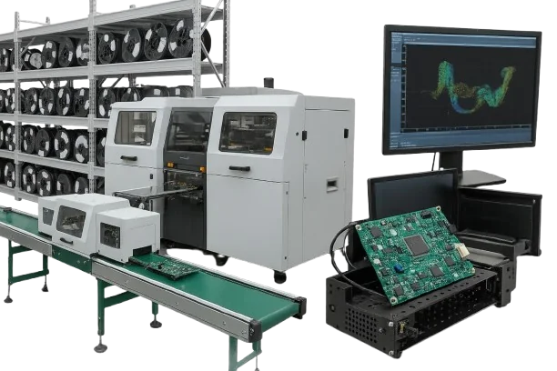
Selective Wave Soldering perfectly resolves this dilemma. It employs a precisely programmable miniature solder nozzle to perform localized soldering only on specific through-hole pins, leaving the rest of the circuit board entirely unaffected by thermal shock. This "surgical" soldering method is particularly crucial for assembling through-hole connectors like SMA, 2.92mm, or SMPM on high-frequency materials such as Rogers PCB, ensuring the integrity of surrounding matching networks and filter circuits. This makes it an ideal choice over traditional through-hole assembly methods.
Millimeter-Wave Interconnect Challenges: From SMA Connectors to Board-Level Soldering Reliability
In millimeter-wave frequency bands, even the slightest impedance mismatch can lead to severe signal reflection and loss. The soldering quality of RF connectors is a critical bottleneck determining interconnect performance. Selective Wave Soldering achieves plump, uniform, and void-free solder joints by precisely controlling solder volume, preheat temperature, and soldering time, ensuring smooth impedance transitions from connectors to PCB traces.
The high repeatability of this process is essential for maintaining performance consistency from the NPI EVT/DVT/PVT (New Product Introduction Engineering/Design/Production Validation Testing) stages to final mass production. During the early NPI EVT/DVT/PVT phases, we must lock in soldering process parameters to ensure that every board produced later replicates the excellent RF performance achieved in the lab.
Key Points of Millimeter-Wave Soldering
- Solder Joint Consistency: Control solder volume and wetting to avoid impedance discontinuities, ensuring phase consistency for beamforming.
- Thermal Stress Control: Protects high-dielectric-constant, low-loss substrates (e.g., PTFE, Rogers) from delamination/warping risks.
- Parasitic Minimization: Reduces residual solder and burrs on pins, minimizing the impact of parasitic L/C on bandwidth and Q-factor.
- PIM Suppression: Enhances the quality of intermetallic compound layers, reducing PIM sources caused by contact nonlinearity.
Key to Fixture Design (ICT/FCT): Ensuring Test Accuracy After Selective Soldering
High-quality assembly relies on rigorous testing validation. The success of selective soldering directly impacts subsequent In-Circuit Testing (ICT) and Functional Testing (FCT). An excellent Fixture design (ICT/FCT) must account for the characteristics of the soldering process. For example, the design of the soldering pallet needs to reserve sufficient contact space for test probes, avoiding interference with solder joints or surrounding components.
At HILPCB, our DFM (Design for Manufacturability) review collaboratively considers soldering and testing requirements. By optimizing component layout, we ensure Selective Wave Soldering proceeds smoothly while guaranteeing stable and accurate contact between Fixture design (ICT/FCT) probes and test points. For early prototypes, we often use Flying Probe Testing for rapid validation, which eliminates the need for expensive fixtures and flexibly detects open or short circuits caused by soldering defects.
DFM/Pallet and Selective Soldering Programming Essentials
- Ensure clearance for nozzle paths and nitrogen hoods; avoid "shadow effects" caused by tall components.
- Add solder dams or no-solder zones between through-holes and nearby impedance traces to mitigate solder wicking risks.
- Select low-thermal-expansion composite materials for pallets; provide probe access windows with chamfers to prevent interference.
- Prioritize preheating and multi-touch strategies for high-thermal-capacity components/ground vias; limit contact time for fine-pin, low-thermal-capacity parts.
- Validate parameters with FAI samples during NPI phases and bind program/fixture version numbers in MES.
Thermal Management and Potting/Encapsulation: Impact of Soldering on PA Heat Dissipation
High-power PAs (Power Amplifiers) are major heat sources in 5G/6G base stations, making their thermal path design critical. Many PA modules dissipate heat through pins or bottom-side thermal pads connected to the PCB's ground layer. The localized heating feature of Selective Wave Soldering effectively avoids excessive thermal shock to the PA chip itself during pin soldering, thereby protecting its delicate internal semiconductor structures.
After welding is completed, Potting/encapsulation is typically performed to enhance the module's weather resistance and mechanical strength. This step requires all solder joints to be flawless, as any rework becomes extremely difficult or even impossible once potting is completed. A reliable selective soldering process is the cornerstone of successful Potting/encapsulation, ensuring long-term electrical connections and structural stability.
HILPCB Assembly Advantages
- Precision Process Control: Programmable nozzle path/height, precise control of solder temperature and nitrogen protection, ensuring stable millimeter-wave solder joint quality.
- DFM/DFA Collaboration: Early design phase involvement, layout adaptation for selective soldering, and reserved space for ICT/FCT fixtures and flying probe testing.
- Full Process Traceability: Traceability/MES records key parameters for each solder joint, providing a data loop for quality analysis and continuous optimization.
- Flexible Testing Solutions: Coverage from Flying probe to customized fixtures (ICT/FCT).
From NPI EVT/DVT/PVT to Mass Production: How Traceability/MES Systems Ensure Soldering Consistency
In the rigorous lifecycle management of communication products, maintaining process consistency from the NPI EVT/DVT/PVT phase to mass production is critical to success. This is where Traceability/MES (Traceability/Manufacturing Execution System) plays a central role. Selective wave soldering equipment integrated with Traceability/MES systems can create a unique identity record for every solder joint on each PCB.
The system records detailed process parameters such as preheat curves, soldering time, and solder temperature. This data is not only used for real-time process monitoring but also enables quick traceability to specific batches, equipment, and operators when issues arise. During the NPI EVT/DVT/PVT phase, this data helps rapidly optimize and solidify the process window. In mass production, the Traceability/MES system becomes a robust backbone ensuring consistent soldering quality across tens of thousands of products, with its data also feeding continuous improvements in Fixture design (ICT/FCT).
Flying Probe Test and Selective Soldering: The Golden Combination for Early Prototype Validation
During the early stages of new product development, iteration speed is crucial. Creating dedicated test fixtures for each prototype version is costly and time-consuming. At this stage, the Flying probe test emerges as the most efficient electrical validation method. It requires no fixtures, using movable probes to directly contact test points, quickly detecting open circuits, short circuits, and component placement errors.
The combination of Flying probe test and Selective wave soldering forms the golden process for prototype/small-batch assembly. Selective soldering achieves through-hole component soldering with near-mass-production quality, ensuring the validity of test results. This allows engineers to identify and resolve soldering-related issues early on, avoiding the discovery of design flaws after investing in costly Fixture design (ICT/FCT) later, thereby significantly shortening the R&D cycle.
In summary, Selective wave soldering is not just a soldering technique but a core enabler for high-performance 5G/6G communication PCB manufacturing. With unparalleled precision, thermal control, and repeatability, it addresses the assembly challenges of high-density, mixed-signal designs in millimeter-wave frequencies. Combined with advanced Fixture design (ICT/FCT), reliable Potting/encapsulation solutions, a Traceability/MES system spanning the entire NPI EVT/DVT/PVT process, and flexible Flying probe test validation, HILPCB provides a one-stop, high-reliability RF assembly solution from prototype to mass production.
Process Window (Typical Range Examples)
| Process/Element | Typical Range | Key Points/Notes |
|---|---|---|
| Flux Type/Solid Content | No-clean or low-residue; solid content 2–8% | Monitor PIM/residues; perform SIR/ionic contamination verification if necessary |
| Preheat Temperature/Time | 90–130°C / 60–120s | Adjust based on board thickness/heat dissipation paths; avoid thermal shock to PTFE/Rogers materials |
Note: The above are general example ranges, not guaranteed values; actual parameters should follow customer specifications/FAI samples/established SOPs and MES programs.
Common Defects × Detection × Prevention (Examples)
| Defect | Detection Method | Prevention/Improvement |
|---|---|---|
| Insufficient hole filling/voids | X-Ray, Cross-section, ICT Resistance | Increase preheat/contact time, optimize via wall metallization, add nitrogen protection |
| Bridging/burrs | Microscopic inspection, AOI, FCT functional anomalies | Reduce nozzle diameter, optimize peel angle and speed, add solder mask dams |
| Solder balls/splashing | Microscopic inspection, cleanliness testing | Adjust flux amount/preheat, optimize path height, add local shielding |
| PIM risk points | PIM testing, S-parameters (return loss/insertion loss) | Improve solder joint quality and contact stability, control residues and surface roughness |
Note: These are typical defect examples and corresponding countermeasures; specific actions should be based on drawings/standards and mass production data, and it is recommended to solidify them into SOP/MES during the FAI stage.
Data and SPC (Example Fields)
| Category | Key Fields | Description |
|---|---|---|
| Welding Process | Program/Fixture Version, Nozzle Diameter, Preheat Curve, Solder Temperature, Contact Time, Nitrogen Concentration | Bound to Board Number/Serial Number; Used for Traceability and SPC Control Charts |
| Electrical/RF Testing | PIM, S-Parameters (S11, S21), Return Loss, Insertion Loss, Tx/Rx Power/Efficiency | Correlated with Welding Batch to Analyze the Impact of Solder Joint Quality on RF Metrics |
| Cleanliness/Reliability | Ionic Contamination (ROSE), SIR, Visual/Microscopic Defects, Post-Reflow Residue | Clean and Retest if Necessary to Avoid PIM/Corrosion Caused by Residue |
Note: SPC recommends establishing X̄-R/Box Plot Alarms for Solder Temperature, Contact Time, Hole Fill Rate, etc.; Out-of-Bounds Conditions Automatically Isolate the Workstation and Trigger Re-inspection.
Test Coverage Matrix (Engineering Sample/Pilot Batch/Mass Production)
| Phase | RF | Electrical | Environmental/Reliability |
|---|---|---|---|
| Engineering Sample (EVT) | Basic S-parameters, PIM sampling if necessary | FPT + Basic FCT | Sample-level thermal cycle/vibration (sampling) |
| Small Batch (DVT) | Full S-parameter coverage + Key PIM points | Stricter ICT/FCT, flying probe supplementary points | Environmental Stress Screening (ESS, sampling) |
| Mass Production (PVT/MP) | Key channel sampling + Online monitoring | Mass production ICT + 100% FCT | High temperature/humidity/salt spray tests per standards |
Note: The matrix is illustrative; final coverage shall comply with customer specifications and regulatory standards. Recommended to solidify in SOP/MES during NPI/FAI phases.
Conclusion
Selective wave soldering achieves a balance between millimeter-wave connectors, thick copper heat dissipation pins, and DFT fixture requirements on the same production line. By leveraging FAI, Flying probe, and Traceability/MES, parameters are locked into each phase of NPI EVT/DVT/PVT, ensuring cross-batch consistency and traceability. Combined with Potting/encapsulation, PIM/S parameter test matrices, and SPC data closed-loop systems, it delivers the optimal solution for 5G/6G RF modules in terms of high-frequency low-loss performance, thermal reliability, and mass-production efficiency.