
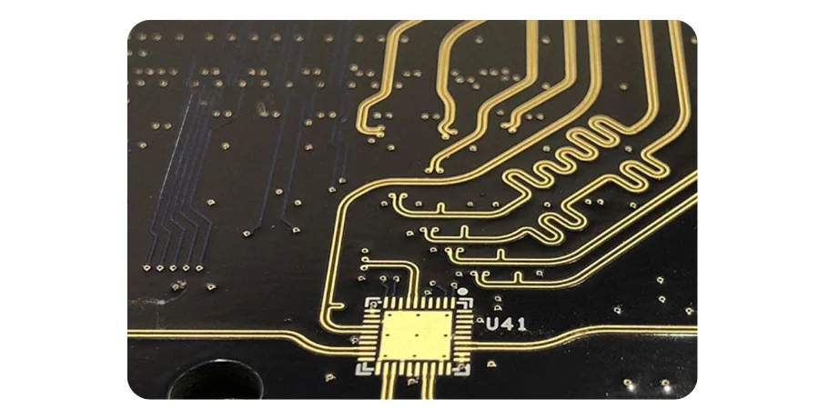
En high-speed digital et RF, la PCB n’est plus seulement un support : elle fait partie du circuit. Quand un signal se propage sur une trace, il “voit” une impédance instantanée : la characteristic impedance. Une Controlled Impedance PCB est une carte dont la géométrie (line width/spacing), le diélectrique (Dk) et le stackup sont maîtrisés pour atteindre un target (ex. 50Ω single-ended, 100Ω differential).
Un mismatch d’impédance crée des reflections, du ringing et de la distorsion, ce qui dégrade fortement la Signal Integrity (SI), notamment pour DDR, PCIe, USB, HDMI. Cette FAQ est structurée autour du keyword what is controlled impedance pcb et couvre 20 questions sur tout le flux (stackup → routing → manufacturing delivery) afin de construire une baseline exécutable.
FAQ overview (20 core questions)
| # | Category | Core question | Key concepts | Quick action |
|---|---|---|---|---|
| 1 | Stackup/Impedance | What is controlled impedance, and why is it required? | Characteristic impedance, reflection | Match source/line/load |
| 2 | Stackup/Impedance | Why does measured impedance differ from simulation? | Dk/Df, etch compensation | Use fab material data + etch factors |
| 3 | Stackup/Impedance | What is Fiber Weave Effect? | Local Dk variation, jitter | Use spread glass, rotate routing |
| 4 | Stackup/Impedance | What happens if a signal crosses a split plane? | Return-path break, EMI | Bridge caps or avoid crossing |
| 5 | Stackup/Impedance | How to choose a reference plane? | GND vs VCC, adjacency | Prefer continuous GND |
| 6 | Layout/Routing | Differential pair fundamentals? | Equal length/spacing, coupling | Maintain symmetry and coupling |
| 7 | Layout/Routing | How tight should length matching be? | Skew | Often < 5 mil; follow datasheet |
| 8 | Layout/Routing | What is a return path? | Minimum-inductance loop | Reference plane adjacent to signal |
| 9 | Layout/Routing | How to optimize high-speed vias? | Via stub, parasitics | Backdrill + GND stitching |
| 10 | Layout/Routing | Serpentine trace: benefits and risks? | Delay tuning, discontinuity | Radius > 3W, spacing > 2W |
| 11 | PI/EMC | How to place decoupling capacitors? | Loop area | Close to pins + via to planes |
| 12 | PI/EMC | Why avoid acute angles? | Acid trap, impedance jump | Use 45° or arcs |
| 13 | PI/EMC | Split ground: good or bad? | Isolation vs return break | Use only when necessary |
| 14 | PI/EMC | How to reduce EMI loop area? | HF current loops | Keep return close to signal |
| 15 | PI/EMC | How to stack power and ground planes? | Plane capacitance, PDN | Tight coupling, ground shielding |
| 16 | Review/Delivery | Why can DRC miss key issues? | Incomplete rules | Build project-based rule templates |
| 17 | Review/Delivery | How to prevent Gerber/BOM/XY mismatch? | Manufacturing errors | Single source + cross-check |
| 18 | Review/Delivery | How to manage ECO effectively? | Version chaos | Formal ECO + version control |
| 19 | Review/Delivery | What is an impedance coupon? | Process verification | Require TDR reports |
| 20 | Review/Delivery | What should DFM review focus on? | Yield & reliability | Pads/vias/spacing/copper limits |
Stackup & impedance
1. Q : Qu’est-ce qu’une controlled impedance PCB et pourquoi c’est indispensable en high-speed ?
- Symptôme : instabilité DDR/PCIe, eye diagram fail, BER élevé.
- Cause : à haute fréquence, la trace est une transmission line. Mismatch → reflections → overshoot/undershoot + ringing.
- Solution : via stackup + géométrie + Dk (width, dielectric thickness vers plane) atteindre 50Ω (SE) / 100Ω (diff).
- Checklist prévention :
- Identifier tôt les nets en impedance control (USB/HDMI/PCIe/DDR).
- Obtenir Dk/Df réels du fabricant PCB.
- Utiliser Polar Si9000 ou impedance calculator (Altium) (voir notre guide du calculateur d’impédance en ligne).
- Documenter targets/tolérances (±10%, critiques ±5%).
2. Q : Pourquoi l’impédance mesurée (TDR coupon) diffère de la simulation ?
- Symptôme : simulation 50Ω, TDR 55Ω.
- Cause :
- Material parameters génériques (Dk/Df).
- Etch compensation non prise en compte (line width diminue).
- Resin flow (dielectric thickness effective change).
- Solution :
- Demander au fab stackup data + etch factors (ex. HILPCB).
- Fournir stackup drawing et exiger build-to-stackup.
- Checklist prévention :
- Confirmer stackup avant routing.
- Mettre un screenshot du modèle d’impédance dans fab notes.
- Exiger coupon + TDR report.
3. Q : Fiber Weave Effect — quel impact sur les signaux très rapides ?
- Symptôme : jitter élevé sur >10Gbps malgré length match.
- Cause : FR-4 = glass weave + resin ; Dk locaux varient → variation de propagation → jitter.
- Solution :
- Spread glass (1067/1086).
- Routing avec angle (10–20°).
- Micro zig-zag (avec prudence).
- Checklist prévention :
- 25Gbps+ : matériaux high-speed (Megtron 6, Rogers 4350B).
- Planifier la direction des bus.
- Demander l’orientation weave si besoin.
4. Q : Que se passe-t-il si une trace traverse un split plane ?
- Symptôme : noise coupling, eye diagram fermé.
- Cause : return path interrompu → grande loop → EMI + SI degradation.
- Solution :
- Éviter crossing (re-layout).
- Si inévitable : bridge capacitor 0.1uF/0.01uF pour return HF.
- Checklist prévention :
- Rules contre cross-split routing.
- Vérifier return path continuity.
- Placer interfaces cross-domain près du boundary.
Piège fréquent : choisir le bon reference plane
Les power planes (VCC) peuvent être noisy ou discontinus. Prefer a continuous ground plane adjacent to the signal layer as the main reference pour une SI stable.
5. Q : Comment choisir le reference plane pour un signal high-speed ?
- Symptôme : le signal se dégrade après un layer change.
- Cause : un bon reference plane est continuous, adjacent, et low-noise (GND).
- Solution :
- Préférer GND (microstrip: plane le plus proche ; stripline: deux planes).
- Ajouter stitching vias près des transitions pour relier les planes et fermer le return path.
- Checklist prévention :
- High-speed layers adjacent à un solid GND.
- DRC rule : stitching vias sur layer change.
- Voir pcb stackup tutorial.
Layout & routing
6. Q : Règles essentielles pour differential pairs ?
- Symptôme : mauvaise immunité, eye opening insuffisant.
- Cause : la performance dépend de la symétrie.
- Solution : equal spacing, equal length, common reference ; minimiser les vias.
7. Q : Quelle tolérance de length matching ?
- Solution : suivre le datasheet ; intra-pair très strict ; inter-pair selon timing budget.
8. Q : Return path — pourquoi c’est critique ?
- Solution : continuous planes, éviter splits/slots, proximité signal-plane.
9. Q : Optimisation des vias pour high-speed ?
- Solution : anti-pad tuning, GND stitching, backdrilling ou blind/buried vias pour réduire via stub.
Need expert support for impedance and stackup design?
HILPCB propose stackup/impedance simulation et via optimization pour augmenter la probabilité de first-pass success.
10. Q : Serpentine trace — bénéfices et risques ?
- Solution : R ≥ 3W, S ≥ 2W, éviter couplage dense, tuning distribué.
Power Integrity & EMC
11. Q : Placement des decoupling capacitors ?
- Solution : minimiser loop area, decaps proches pins, via vers planes, multi-value (0.1µF/0.01µF/100pF).
12. Q : Pourquoi éviter les angles aigus ?
- Cause : acid trap (fab) + impedance step (SI/RF).
- Solution : 45° ou arcs.
13. Q : Split ground — bon ou mauvais ?
- Solution : préférer single solid GND plane + zoning ; split seulement si nécessaire (ADC/DAC, safety isolation).
14. Q : Réduire EMI loop area ?
- Solution : return path serré, decoupling, clocks/switch nodes courts, shielding/via fence.
15. Q : Stack power/ground planes ?
- Solution : tight coupling (plane capacitance), GND shielding, power plane pullback (20H).
Review & delivery
16. Q : DRC “No Violations” mais problèmes réels ?
- Solution : règles complètes + sync avec capability fab + manual review.
17. Q : Éviter mismatch Gerber/BOM/XY ?
- Solution : single source outputs, batch export, cross-check.
18. Q : Gestion ECO ?
- Solution : ECO flow, version control, docs sync.
19. Q : Impedance coupon ?
- Solution : exiger coupon + TDR report ; vérifier tolérances.
20. Q : Focus DFM ?
- Solution : min features/drill, via strategy, SMT spacing/silk/mask, panelization.
DFM & delivery checklist
| Area | Check item | Requirement | Owner |
|---|---|---|---|
| Schematic | Library consistency | All parts from validated central library | Designer |
| ERC | No floating pins / power conflicts | Designer | |
| BOM completeness | Full refdes/PN/footprint/description | Designer | |
| Stackup/Impedance | Stackup confirmation | Material/thickness/Dk/Df confirmed with fab | Design/Process |
| Impedance rules | All controlled nets have correct rules | Designer | |
| Plane continuity | No splits/large voids under HS nets | Designer | |
| Placement | Modular placement | Digital/analog/power/RF clearly separated | Designer |
| Critical placement | Decaps, crystals, connectors optimized | Designer | |
| Thermal | Heatsources have copper/vias/space | Designer | |
| Manufacturable spacing | Component-to-component/edge spacing OK | Designer | |
| Routing | Power nets | Short and wide power, solid ground | Designer |
| High-speed | Diff pairs/clocks follow constraints | Designer | |
| Length match | All length matching met and recorded | Designer | |
| Via optimization | GND stitching, no stub risk on key nets | Designer | |
| Acute angles/copper islands | No acute corners; no floating copper | Designer | |
| Silk/Assembly | Silkscreen clarity | Refdes visible; orientation clear | Designer |
| Polarity | Clear polarity markers for diodes/caps/ICs | Designer | |
| Fiducials | ≥3 fiducials, L-shape distribution | Designer | |
| Production files | Gerbers | Correct layer order, RS-274X | Designer |
| Drill files | Size/plating correct, aligned to Gerbers | Designer | |
| BOM | Matches schematic + PCB | Designer | |
| XY | Origin/unit/rotation correct | Designer | |
| Fab notes | Material, thickness, impedance, finish, etc. | Designer | |
| Final review | DFM review | Fab or senior engineer final check | Process/External |
| Version control | All outputs from locked release | Designer |
Recommended learning path
Ressources recommandées : Bogatin (Signal Integrity Simplified), Howard Johnson (High-Speed Digital Design), IPC-2152/IPC-2221, outils (impedance/length/3D), formations SI/PI/EMC.
De la conception à la fabrication : HILPCB comme partenaire
Comprendre “what is controlled impedance pcb” est le premier pas. HILPCB propose free DFM review, services stackup/impedance et TDR reports pour controlled impedance PCBs.
Prêt pour votre prochain projet high-speed PCB ? Contactez notre équipe pour un devis et une consultation gratuite.
Conclusion
Cette FAQ fournit une baseline opérationnelle autour de what is controlled impedance pcb, avec réponses et checklists. En appliquant ces points et en impliquant tôt l’équipe DFM/DFA de HILPCB, vous accélérez prototype → production tout en conservant qualité et compliance.
Support : HILPCB Turnkey Assembly ou SMT Assembly.
Questions fréquentes
Qu’est-ce qu’un controlled impedance PCB ?
C’est une carte où la géométrie des pistes, le diélectrique et le stackup sont maîtrisés pour atteindre une impédance caractéristique cible.
Pourquoi l’impédance contrôlée est-elle importante en pratique ?
Elle réduit les réflexions, le ringing et les distorsions sur les signaux high-speed ou RF, ce qui améliore la signal integrity.
Pourquoi l’impédance mesurée peut-elle différer de la simulation ?
Les tolérances de fabrication, les vraies propriétés matière, les effets d’etch et les variations de stackup peuvent modifier la valeur finale.
Que faut-il maîtriser en premier pour obtenir un résultat fiable ?
Il faut aligner tôt le stackup, les plans de référence, les règles de routage et la capacité du fabricant, puis confirmer avec DFM et test.