
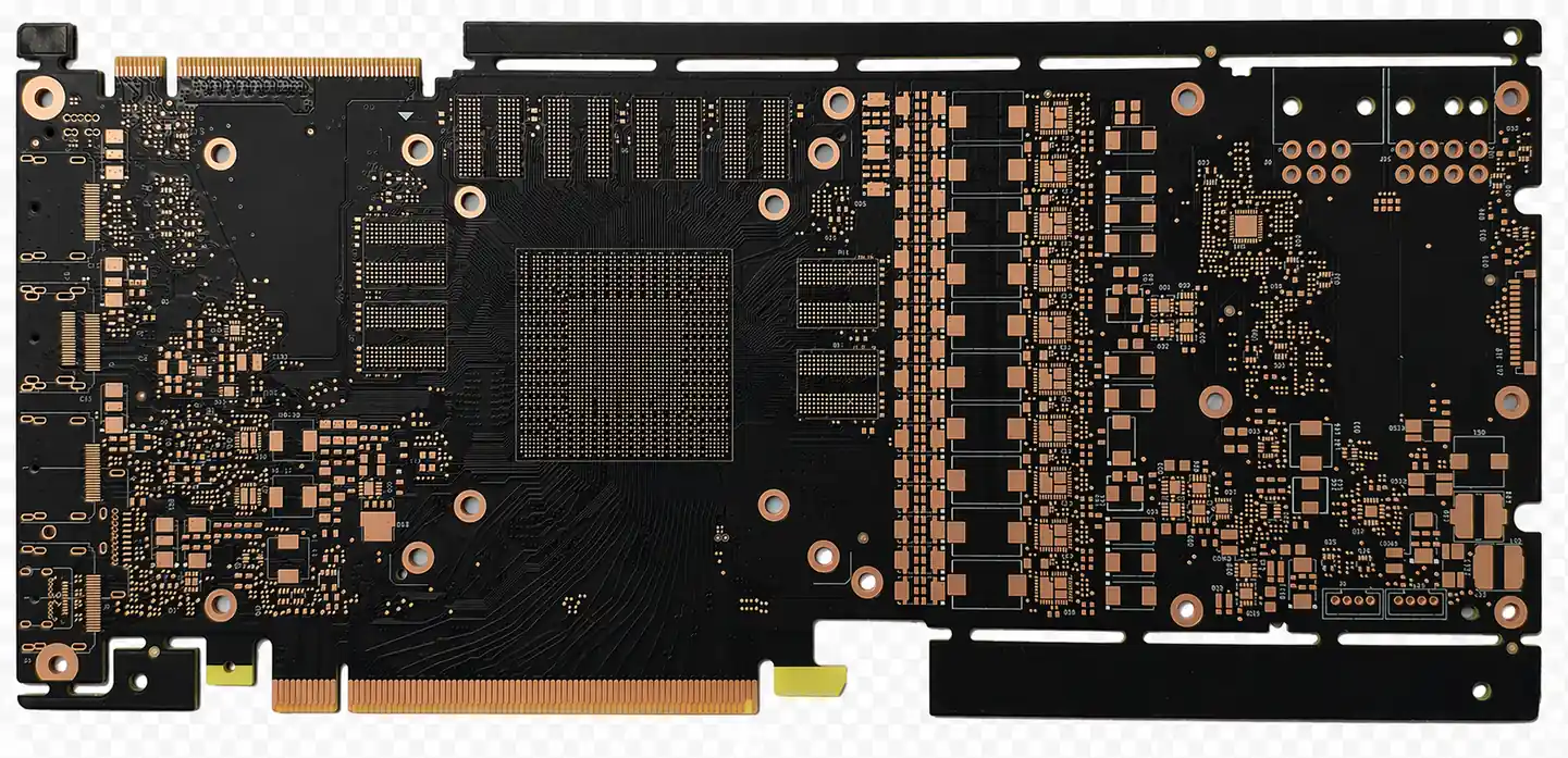
A 24-layer PCB is a multilayer printed board with 24 patterned copper layers separated by laminate cores and prepregs, then bonded into one controlled construction. It can provide the routing density, reference planes, power distribution, and shielding needed by servers, switches, backplanes, telecom systems, and high-end instrumentation, but 24 layers do not automatically deliver 112G signal integrity.
For high-speed hardware, the production challenge is correlation: the fabricated board must preserve the geometry, material behavior, copper profile, via transition, and measurement reference plane assumed by the electrical model.
Key Takeaways
- Select 24 layers from a layer-budget and escape study. Protocol names, aggregate bandwidth, or board prestige are not valid layer-count rules.
- A 24-layer board can use one main lamination cycle or multiple sequential cycles. HDI and buried-via architecture—not copper-layer count alone—sets the lamination plan.
- PAM4 carries two bits per symbol. A nominal 112 Gb/s PAM4 lane operates near 56 GBd and has a Nyquist frequency near 28 GHz, but its exact channel limits come from the applicable interface specification.
- Low-loss resin is only part of the channel. Glass construction, resin content, copper profile, bonding treatment, trace geometry, vias, connectors, and launches also affect loss and skew.
- Backdrill requirements must come from the modeled via transition and residual-stub budget. “112G always means a 6 mil stub” is not a universal rule.
- VNA data are meaningful only when the coupon, fixture, calibration, de-embedding, reference impedance, bandwidth, sampling, and acceptance metric are defined.
- Freeze material construction and process variables between first article and production. A nominally equivalent laminate or foil change can invalidate correlation.
Table of Contents
- When is a 24-layer PCB the right architecture?
- How should a 24-layer stackup be planned?
- What does 112G PAM4 change for fabrication?
- How should low-loss materials and copper be selected?
- Does a 24-layer PCB require sequential lamination?
- How should vias and backdrilling be designed?
- Where do 24-layer boards fail in manufacturing?
- How can simulation and production be correlated?
- How should insertion loss be measured?
- What must be frozen after first article approval?
- What controls 24-layer PCB cost and yield?
- What should a 24-layer PCB RFQ include?
When Is a 24-Layer PCB the Right Architecture?
A 24-layer construction is justified when the board cannot meet placement, routing, reference, power, isolation, loss, or mechanical requirements with fewer layers at acceptable risk. Start with a layer budget rather than copying a server stackup.
| Design demand | Why 24 layers may help | Required evidence |
|---|---|---|
| Large CPU, GPU, FPGA, switch, or accelerator packages | More signal layers can support dense escape and channel fan-out | Package breakout study, via map, routing utilization, and assembly keepouts |
| Many serial lanes | Dedicated stripline layers and reference planes can control return paths and crosstalk | Lane map, reach class, channel budget, transition count, connector/cable topology |
| Wide memory interfaces | More routing layers can preserve byte-lane topology and reference continuity | Controller/memory vendor rules, timing budget, topology, layer-transition plan |
| Complex PDN | Additional plane area can distribute multiple rails and reduce shared-path impedance | Rail map, current/transient budget, target impedance, decoupling and plane-resonance analysis |
| Backplane or large-format board | More layers can separate long routes, connector fields, management, and power | Board dimensions, press-fit constraints, channel model, mechanical and bow/twist limits |
| Mixed RF and digital functions | Functional layer groups can isolate routing and references | Frequency plan, coupling limits, material compatibility, shielding and grounding strategy |
| Safety or functional isolation | More copper layers can support routing while preserving boundaries | Creepage/clearance, slotting, insulation system, applicable safety standard and system test |
Layer count is not a quality grade. Adding layers can increase registration, resin-flow, drill, plating, coupon, panel-utilization, and change-control risks. If a 20-layer stackup meets the same evidence with wider process margins, it may be the stronger production architecture.
Applications That Commonly Reach 24 Layers
High-layer-count boards appear in server motherboards, AI accelerator carrier boards, network switch line cards, optical transport systems, backplane PCB assemblies, imaging and data-acquisition platforms, and some aerospace or defense electronics. The end market does not define the stackup; package density, channel reach, power, environment, standards, and lifecycle do.
How Should a 24-Layer Stackup Be Planned?
A practical stackup gives each critical signal a controlled reference, distributes power without creating return-path gaps, uses manufacturable trace dimensions, and balances copper and dielectric about the centerline.
The following map is a functional example only. It deliberately omits dielectric and trace dimensions because those must come from the selected fabricator's material constructions and field solver.
| Layer | Example function | Layer | Example function |
|---|---|---|---|
| L1 | Surface components and signals | L24 | Surface components and signals |
| L2 | Ground reference | L23 | Ground reference |
| L3 | High-speed signal | L22 | High-speed signal |
| L4 | Ground reference | L21 | Ground reference |
| L5 | High-speed signal | L20 | High-speed signal |
| L6 | Power plane | L19 | Power plane |
| L7 | General/high-speed signal | L18 | General/high-speed signal |
| L8 | Ground reference | L17 | Ground reference |
| L9 | Memory/general signal | L16 | Memory/general signal |
| L10 | Power plane | L15 | Power plane |
| L11 | General signal | L14 | General signal |
| L12 | Ground reference | L13 | Ground reference |
This S-G-S-G-S-P-S-G-S-P-S-G / G-S-P-S-G-S-P-S-G-S-G-S pattern provides 12 signal layers, eight ground layers, and four power layers. A real board may allocate more power planes, fewer routing layers, dual-reference stripline, build-up layers, hybrid materials, or different center planes.
Stackup Questions to Resolve Before Routing
- Which interfaces use each signal layer, and what is the adjacent reference on both sides?
- What impedance, loss, crosstalk, skew, and reference-continuity requirements apply to each route class?
- Can the factory achieve useful trace widths and spacing with stocked cores, prepregs, copper, and glass constructions?
- Which power planes may be split, and can any critical signal cross those boundaries?
- Does the finished thickness support the required plated-hole aspect ratio, connector engagement, stiffness, and enclosure fit?
- Are copper distribution, resin demand, and dielectric construction balanced enough for lamination and bow/twist control?
- Which vias require PTH, blind, buried, microvia, via-in-pad, fill, cap, or backdrill processing?
- Can all required coupons, tooling, rails, and test structures fit the production panel?
Use the production stackup—not a generic web calculator—as the single source of truth. A change to cured prepreg thickness can alter impedance, overall thickness, via depth, residual stub, and registration margin at the same time.
What Does 112G PAM4 Change for Fabrication?
PAM4 uses four amplitude levels and carries two bits per symbol. A nominal 112 Gb/s lane is therefore near 56 GBd, giving a Nyquist frequency near 28 GHz. Actual signaling rates, reach classes, channel masks, test points, equalization, FEC, and compliance methods depend on the governing interface, such as an OIF CEI-112G implementation agreement or IEEE 802.3 electrical interface.
The ideal spacing between PAM4 levels is one-third of the full level range, but finished-system margin is not simply “one-third of NRZ.” Transmitter noise, receiver architecture, equalization, jitter, crosstalk, reflections, linearity, coding, and test methodology all contribute. Fabricators should not turn a modulation summary into an unsupported universal loss or impedance limit.
Translate the Channel Specification Into Fabrication Controls
| Electrical concern | Fabrication variable | Contractable evidence |
|---|---|---|
| Insertion loss | Df, copper profile, bonding treatment, trace geometry, route length | Defined loss coupon and frequency-domain measurement |
| Return loss | Impedance geometry, etch, via/anti-pad, launch, connector field | TDR plus S-parameter structure where required |
| Differential-to-common-mode conversion | Pair symmetry, weave exposure, via/return geometry, skew | Mixed-mode S-parameters or validated transition coupon |
| Crosstalk | Layer spacing, trace separation, broadside geometry, via field | Field-solver rule plus optional crosstalk coupon |
| Propagation delay/skew | Dk distribution, glass weave, path geometry, pair length | Construction control and delay/skew measurement if contracted |
| Lot-to-lot drift | Material lot, press result, copper treatment, etch and plating | Traceability, SPC, coupon trend and change notice |
The PCB is one segment of the complete channel. Package, breakout, AC-coupling components, connectors, retimers, cables, and receiver/transmitter equalization consume the same system margin. A bare-board coupon cannot certify protocol compliance by itself.
How Should Low-Loss Materials and Copper Be Selected?
Select the material system from a channel and reliability budget, then confirm that the intended factory can source and process the exact constructions. A family name without glass style, resin content, copper option, thickness, and test method is incomplete.
Material Selection Evidence
| Property | Why it matters on 24 layers | What to verify |
|---|---|---|
| Dk versus frequency | Sets impedance geometry and propagation delay | Test method, frequency, construction-specific value, model used by field solver |
| Df versus frequency | Contributes to dielectric loss | Same method/frequency basis used in the channel model |
| Glass style and resin content | Affect cured thickness, local Dk, skew, resin flow, and registration | Available constructions and spread/square-weave options |
| Tg, Td, Z-axis CTE, T260/T288 | Affect multiple reflow/lamination and plated-hole stress | Datasheet method plus application qualification |
| Copper profile | Changes conductor loss and adhesion/process behavior | Foil designation, side-specific roughness parameters, supplier and treatment |
| CAF and moisture behavior | Matter in dense via fields and harsh environments | Qualification basis, spacing, bias, humidity and test plan |
| Availability and alternates | Affect prototype-to-production continuity | Stocked constructions, minimum order, approved substitution list and notice |
Isola's December 2025 I-Tera MT40 data sheet provides a useful example of complete context: it lists Dk 3.45 and Df 0.0031 with stated test methods, offers mechanically spread glass and HVLP foil at no more than 2.5 µm Rz JIS for listed options, and reports multiple-lamination-cycle compatibility. These are typical material data, not guarantees of finished-channel loss.
Panasonic positions MEGTRON 6 and MEGTRON 7 as low-loss materials for high-speed, high-layer-count networking and server applications, with different glass and copper options. The design team should request the current construction data from the actual supply chain instead of copying one Dk/Df pair from a secondary comparison table.
Copper Roughness and Bonding Treatment
At tens of gigahertz, current is concentrated near conductor surfaces, and roughness can increase conductor loss. Yet “VLP” and “HVLP” are category labels, not a complete electromagnetic model. Confirm which surface touches the dielectric, which roughness metric is reported, and how the inner-layer bonding treatment changes that surface.
A low-profile foil can lose part of its electrical benefit if the bonding process adds significant texture. Conversely, the smoothest foil is not automatically the best choice if peel strength, thermal cycling, fine-line etch, availability, or qualification suffers. Model and qualify the complete copper-resin-treatment system.
Glass-Weave Skew
Woven glass creates local dielectric variation. A differential pair whose legs see different glass/resin distributions can develop skew and mode conversion. Mechanically spread glass, suitable construction choice, routing angle, and wider pair-to-weave averaging can reduce risk, but no universal angle or glass style guarantees compliance. Review actual artwork orientation, panel grain direction, trace length, and material construction.
Does a 24-Layer PCB Require Sequential Lamination?
No. A conventional 24-layer plated-through-hole board can be built by laminating patterned cores and prepregs in one main multilayer press cycle. Sequential lamination becomes necessary when the interconnect architecture includes buried vias, build-up microvias, stacked structures, or another feature that must be formed and plated before later layers are added.
| Build architecture | Typical lamination implication | Key risk |
|---|---|---|
| PTH-only 24-layer rigid board | One main multilayer lamination may be possible | Thick-board drill/plating aspect ratio, registration and via stubs |
| PTH plus backdrill | Main lamination plus secondary controlled-depth drilling | Stub tolerance, target-pad protection and keepout |
| Buried-via subcomposite | At least one sub-lamination before final lamination | Subcomposite scaling, registration accumulation and trapped defects |
| 1+22+1 HDI | Build-up layers added around a 22-layer core | Laser-via capture, fill, cap, sequential registration and reflow reliability |
| Stacked microvia architecture | Multiple repeated build-up operations | Interface stress, voids, copper fill and qualification limits |
| Hybrid RF/digital stack | May be single or multiple cycle depending on construction | Cure compatibility, CTE, resin flow, bond treatment and material movement |
Each additional cycle reheats existing structures and creates another scaling and registration event. Do not specify sequential lamination because “24 layers are advanced.” Specify it only when the via and material architecture requires it.
An HDI PCB can solve fine-pitch escape and shorten transitions, but it is not a free signal-integrity upgrade. The release package must define microvia depth, land, dielectric, stacking/staggering, fill, cap, inspection, and reliability requirements.
How Should Vias and Backdrilling Be Designed?
On a thick high-layer board, a via transition can dominate local return loss and mode conversion. Its behavior depends on barrel length, stub length, pad and anti-pad geometry, reference transitions, return vias, drill/plating variation, and nearby structures.
Choose the Interconnect From the Transition, Not the Data Rate
| Transition condition | Candidate architecture | Required analysis |
|---|---|---|
| Signal uses nearly the full PTH barrel | PTH without backdrill may be adequate | Exact production stub and full transition model |
| Surface-to-shallow-inner transition leaves long barrel | Backdrill or blind via | Compare residual stub, clearance, cost, reliability, and loss |
| Dense BGA escape with limited secondary-drill clearance | Laser microvia or layer reassignment | Package escape and HDI qualification |
| Connector pin must remain mechanically intact | PTH/backdrill coordinated with press-fit design | Pin engagement, remaining barrel and launch model |
| Different net classes stop on several layers | Multiple backdrill depth classes | Layer-referenced drill table and CAM attribute audit |
| Transition changes reference planes | Signal via plus intentional return transition | 3D model of signal, references, return vias and anti-pads |
Backdrilling removes unused plated barrel with a larger controlled-depth drill after plating. The approved drawing should state drill side, target layer or depth convention, secondary diameter, maximum residual stub, no-drill safety allowance, affected net or via class, and inspection method.
Do not prescribe one residual-stub value for every 112G implementation. The design owner should derive the limit from the applicable channel specification and transition model. The fabricator should then return achievable depth tolerance and a cross-section plan based on the production stackup.
Return vias also require analysis. A fixed count or fixed 20 mil distance can be wrong when the reference nets, pitch, anti-pads, connector geometry, or bandwidth changes. Preserve symmetry where the interface requires it and model the complete return path.
Where Do 24-Layer Boards Fail in Manufacturing?
High layer count amplifies interactions between material movement, copper distribution, resin flow, drilling, plating, and measurement. The failure-mode table should be reviewed during DFM, not after a failed lot.
| Failure mode | Common mechanism | Prevention and evidence |
|---|---|---|
| Inner-layer misregistration | Scaling error, material movement, tooling and lamination variation | Fabricator compensation model, targets, X-ray/optical data and microsection |
| Resin starvation or voids | High local copper, insufficient resin, poor flow or trapped gas | Copper-density review, construction selection, lamination control and sectioning |
| Excessive thickness drift | Cured prepreg variation, copper distribution and press result | Production stackup control and measured coupon/cross-section thickness |
| Bow and twist | Asymmetric copper/dielectric, uneven stress, large format | Balanced construction, panel design, agreed method and acceptance limit |
| PTH barrel void/crack | Desmear, plating distribution, small hole and thermal stress | Aspect-ratio review, process coupons, thermal stress and microsection |
| Annular-ring breakout | Registration stack plus small lands and drill movement | Manufacturable lands, target data and invoked IPC acceptance criteria |
| Backdrill target damage | Depth convention error, panel thickness drift or drill variation | First-article sections and layer-referenced drill control |
| Excess residual stub | Conservative depth, wrong buildup or calibration | Contracted limit and measured section or suitable metrology |
| Impedance drift | Etch, copper thickness, dielectric thickness, Dk or mask variation | Production solver geometry, TDR coupons and SPC |
| Loss drift | Material/foil/treatment lot, trace geometry or coupon/fixture change | Controlled loss coupon, traceability and measurement-system control |
| CAF or insulation failure | Moisture, contamination, spacing, material and bias-temperature stress | Application-specific design and qualification plan |
| Latent HDI failure | Microvia interface stress, void, weak fill/cap or stacked structure | Qualified structure, microsection and appropriate reliability testing |
Electrical opens/shorts testing cannot detect most of these risks. Inspection and test must be chosen for the failure mechanism.
How Can Simulation and Production Be Correlated?
Correlation means proving that the physical variables used in the model are represented by the fabricated board and measurement. It does not mean adjusting a simulated curve until it resembles one coupon.
Model-Control-Evidence Matrix
This matrix is a practical release asset for high-speed NPI. It connects each model input to a production control, a measurement, and a response if the data move.
| Model input | Production control | Evidence | If correlation drifts |
|---|---|---|---|
| Cured dielectric thickness | Exact core/prepreg construction and press process | Cross-section or controlled stackup measurement | Recalculate impedance/loss; investigate material and lamination lot |
| Dk versus frequency | Approved material, glass style and resin content | Delay/phase extraction or supplier construction data | Update model only after ruling out geometry/fixture error |
| Df versus frequency | Material lot, moisture and process control | De-embedded loss measurement | Separate dielectric, conductor and fixture contributions before disposition |
| Copper width/thickness | Artwork compensation, etch and plating | Cross-section and line-width metrology | Correct process or model with approved production geometry |
| Copper roughness | Approved foil side/profile and bonding treatment | Supplier certificate plus optional profilometry | Block unapproved foil/treatment substitution; rerun channel analysis |
| Via barrel/stub | Drill, plating, backdrill program and stackup | Microsection or qualified nondestructive method | Check depth convention, panel thickness and tool calibration |
| Pad/anti-pad registration | Layer scaling and drill alignment | X-ray/target data and section | Reassess transition distribution, not just nominal model |
| Coupon launch/fixture | Controlled artwork, connector/probe and setup | Calibration/de-embedding validation | Fix measurement system before changing product disposition |
Use at least two correlation levels:
- First article characterization: establish actual geometry, impedance, loss, transition behavior, material traceability, and measurement repeatability.
- Production monitoring: measure the smallest set of variables that detects meaningful drift, with agreed control limits and escalation rules.
Not every production panel needs a laboratory-scale full-channel characterization. The right sampling plan depends on risk, process capability, lot definition, measurement repeatability, contract requirements, and the cost of an escape.
How Should Insertion Loss Be Measured?
“VNA tested to 40 GHz” is incomplete. The frequency limit alone does not establish accuracy, coupon relevance, or acceptance.
Define the Measurement Contract
- measured structure: uniform trace, via transition, crosstalk pair, connector launch, or complete channel surrogate
- signal format: single-ended or differential; required mixed-mode S-parameters
- coupon layer, geometry, length pair, reference planes, surface finish, solder mask, and panel location
- ports, probes or connectors, cable/fixture arrangement, reference impedance, and calibration plane
- calibration/de-embedding method such as TRL, 2X-Thru, or another validated method
- frequency range, point spacing, IF bandwidth, averaging, time-domain gating, smoothing, and file format
- metric and limit: raw/fitted insertion loss, loss per unit length, return loss, mode conversion, delay, or another specified value
- sampling by panel/lot, repeatability check, golden/reference coupon, disposition, raw-data retention, and traceability
IPC-TM-650 2.5.5.12A describes five printed-board signal-loss methods, including time- and frequency-domain approaches. IPC-TM-650 2.5.5.14 focuses on frequency-domain loss and propagation measurement, including coupon design, calibration, TRL, 2X-Thru, and de-embedding. IEEE 370-2020 provides practices for high-quality PCB interconnect S-parameter measurement validated up to 50 GHz.
These documents help define a method; they do not supply the product's acceptance limit. The interface owner must set limits from the channel allocation and specify the test point and reference plane.
Match Coupon Purpose to Decision
| Coupon | Useful decision | What it does not prove |
|---|---|---|
| TDR impedance coupon | Is characteristic impedance within the contracted range? | Broadband channel loss or protocol compliance |
| Two-length trace coupon | What is de-embedded propagation loss/delay per length? | Product via, connector or BGA launch behavior |
| Via transition coupon | Does the manufactured transition resemble the modeled S-parameters? | Every product via if geometry or surroundings differ |
| Crosstalk coupon | Does a specified spacing/layer arrangement meet a coupling limit? | Different routing neighborhoods or connector fields |
| Material characterization coupon | Can Dk/Df or propagation behavior be extracted for model correlation? | Full product performance without geometry correlation |
The image above can represent a loss-coupon concept, but publication should not label it as a specific HILPCB measurement, frequency, material, or production result without verified provenance.
What Must Be Frozen After First Article Approval?
The first article is useful only if production preserves the variables that made it pass. Create an approved product/process baseline and require written review before changing any channel-sensitive item.
| Freeze item | Why a change matters | Required response |
|---|---|---|
| Laminate family and construction | Dk/Df, cured thickness, resin flow and reliability may change | Customer approval plus model/test impact review |
| Glass style and resin content | Impedance, delay, weave skew and thickness may change | Recalculate and correlate affected layers |
| Copper supplier/profile/side | Conductor loss and adhesion behavior may change | Review roughness model and loss evidence |
| Bonding treatment | Can alter roughness, adhesion and processing | Qualification and loss-correlation review |
| Stackup and finished thickness | Changes impedance, via length, stub and mechanical fit | New controlled stackup and electrical review |
| Trace compensation and finished copper | Changes impedance and loss | Re-solve geometries and verify coupons |
| Drill/backdrill program | Changes transition and reliability | Updated drill table, section and SI review |
| Lamination route or press cycle | Changes material movement, registration and thermal history | Process requalification as required |
| Coupon artwork or panel position | Breaks trend continuity | Establish correlation before replacing baseline |
| VNA fixture, probe, calibration or software | Can shift measured results without product change | Measurement-system correlation and validation |
| Fabrication site or major equipment route | Process capability may differ | Transfer plan, first article and agreed validation |
Record deviation authority, change-notice period, containment, requalification triggers, and who can approve a temporary substitution. “Equivalent material” is not an electrical engineering conclusion until equivalence criteria are defined.
What Controls 24-Layer PCB Cost and Yield?
The quote reflects much more than 24 sheets of copper. The main drivers are risk, panel economics, material, process cycles, feature margin, and evidence.
- Board and panel size: large server or backplane formats can fit only a small number of boards per panel; coupons and rails consume additional area.
- Low-loss material system: premium resin, spread glass, low-profile foil, stocked constructions, and lot traceability affect material and procurement cost.
- Copper distribution and layer count: high copper imbalance can demand additional engineering and reduce lamination margin.
- Via architecture: small PTHs, high aspect ratios, buried vias, laser microvias, fill/cap, stacked structures, and backdrill depth classes add risk and operations.
- Sequential lamination: each added cycle increases handling, registration events, inspection, thermal history, and cycle time.
- Fine geometry and tight tolerances: narrow lines, small lands, tight impedance, depth, thickness, or registration limits can lower yield.
- Drill volume and classes: large hit counts, many tool sizes, two-side backdrill, and press-fit fields consume machine time and tooling.
- Test structures and reports: TDR, loss, via, crosstalk, microsection, material, reliability, first-article, and raw-data requirements use panel and engineering resources.
- Traceability and change control: controlled lots, certificates, retained samples, site restrictions, and requalification requirements add governance cost but reduce lifecycle uncertainty.
Reduce cost by increasing process margin, improving panel utilization, consolidating truly equivalent structures, and using characterization only where it resolves a decision. Do not remove traceability or tests that protect an expensive system-level failure.
What Should a 24-Layer PCB RFQ Include?
Product and design data
- ODB++, IPC-2581, Gerber X2, or another agreed fabrication dataset, plus netlist and fabrication drawing
- exact layer order/function, reference-net map, plane splits, impedance/loss classes, and channel-critical net identification
- NC drill/route files, via start-stop definitions, pad/anti-pad, fill/cap, backdrill side/target/diameter/stub limit, and press-fit details
- board and array dimensions, finished thickness, copper definition, finish, mask, legend, edge, connector, stiffener, and mechanical requirements
- package escape, connector launch, channel model or sensitivity information needed for DFM without disclosing unnecessary IP
Material and electrical data
- approved laminate families/constructions or performance requirements, glass style, resin content, Dk/Df basis, Tg/Td/CTE, CAF/moisture and compliance needs
- copper weight, profile/roughness, foil side, bonding-treatment requirements, and approved alternates
- impedance nominal/tolerance by structure, mask condition, trace geometry ownership, coupon correlation, and TDR report requirements
- insertion/return-loss, mode-conversion, crosstalk, or delay limits with frequency, reference plane, coupon, de-embedding and raw-data format
- signal standards/reach classes, power/current, voltage/isolation, thermal, environmental, lifecycle and reliability requirements that affect the bare board
Quality, change, and commercial data
- invoked IPC revisions, performance class, addenda, customer specifications, deviations and precedence
- inner AOI, netlist test, registration, microsection, thermal stress, backdrill, TDR, VNA, dimensions, bow/twist, cleanliness and material evidence
- first-article plan, qualification versus lot acceptance, sampling, lot definition, traceability, data retention, deviation approval and requalification triggers
- prototype and production quantities, forecast, panel/array quantities, target delivery, destination, packaging and optional assembly/sourcing scope
- controlled variables and written change-notice requirements from the approved first article baseline
HILPCB can review a 24-layer high-speed PCB package for stackup, material, impedance, loss coupons, via/backdrill, HDI, fabrication, assembly, test, traceability, and change-control planning. Actual capability, tolerance, material, panel size, certification, test bandwidth, sampling, and lead time must be confirmed for the quoted construction.
Standards and Responsibility Scope
Common references include:
- IPC-2221C — Generic Standard on Printed Board Design
- IPC-2226 — Sectional Design Standard for High Density Interconnect Printed Boards
- IPC-6012E — Qualification and Performance Specification for Rigid Printed Boards
- IPC-4101 — Specification for Base Materials for Rigid and Multilayer Printed Boards
- IPC-TM-650 2.5.5.7 — Characteristic Impedance of Lines on Printed Boards by TDR
- IPC-TM-650 2.5.5.12A — Test Methods to Determine the Amount of Signal Loss on Printed Boards
- IPC-TM-650 2.5.5.14 — Measuring High Frequency Signal Loss and Propagation on Printed Boards with Frequency Domain Methods
- IEEE 370-2020 — Electrical Characterization of Printed Circuit Board and Related Interconnects at Frequencies up to 50 GHz
- OIF CEI-112G implementation agreements — applicable 112G electrical reach and interface requirements
- IEEE 802.3ck — 100 Gb/s, 200 Gb/s, and 400 Gb/s electrical interfaces
The contract must state revision, class, addendum, interface/reach clause, test point, metric, frequency, sampling, limits, and precedence. A list of standards without these details is not an acceptance plan.
HILPCB's responsibility is limited to the fabrication, assembly, sourcing, inspection, documentation, measurement, and change-control scope accepted in writing. The customer owns silicon selection, architecture, channel allocation, equalization, signal/power/thermal models, safety, firmware, connector/cable/enclosure behavior, qualification, regulatory compliance, and finished-system validation unless reassigned by contract.
Common Questions
Is every 24-layer PCB a sequential-lamination board?
No. PTH-only 24-layer boards may use one main multilayer lamination. Buried vias, HDI build-up layers, or other staged interconnects create the need for sequential cycles.
Does 112G PAM4 always require 24 layers?
No. Layer count follows routing density, package escape, references, power and mechanics. A smaller board may route a few 112G lanes on fewer layers, while a dense switch or accelerator board may need more than 24.
Is the Nyquist frequency of a 112 Gb/s PAM4 lane 28 GHz?
Approximately, for a nominal 112 Gb/s lane carrying two bits per PAM4 symbol: about 56 GBd and 28 GHz Nyquist. Use the exact signaling rate and channel definition from the applicable specification.
Is MEGTRON 6, MEGTRON 7, or I-Tera MT40 automatically required?
No single laminate is mandatory for every channel. Model the entire route, compare current construction data, confirm factory availability and process qualification, and select the material that meets electrical and reliability margin.
Must every 112G signal via be backdrilled?
No. Backdrill is driven by the unused plated stub and transition model. A via that traverses most of the stackup, a blind via, or a short acceptable stub may not need it.
Does a TDR impedance pass prove insertion loss?
No. TDR impedance and broadband insertion loss answer different questions. Use a defined loss coupon and validated frequency-domain method when loss is a contractual requirement.
What makes VNA coupon data trustworthy?
The coupon must represent the intended layer and process, and the test must define fixture, calibration, de-embedding, reference plane, impedance, bandwidth, settings, repeatability, metric, limit, sampling, and raw-data retention.
What is the most important production control after first article?
Prevent unreviewed changes to the material construction, glass, copper profile, bonding treatment, stackup, drill/backdrill route, coupon, fabrication site, and measurement system.
Build a Measurable 24-Layer Release Package
A high-speed 24-layer board is ready for production only when the electrical model, physical construction, process controls, coupon structures, measurement reference planes, acceptance limits, and change authority describe the same product.
For a construction-specific review and quotation, send HILPCB the 24-layer PCB package with the stackup, channel classes, materials, via/backdrill table, quantities, test plan, and first-article evidence requirements.