
High-Speed Backplane PCB Manufacturing | Up to 64 Layers | Data Center & Telecom Solutions
Manufacturing 64-layer high-speed backplane PCB systems with 25+ Gbps channels, large 600 × 800 mm panels, precision back-drilling, and impedance control within ±3%. Trusted for telecom, data center, aerospace, and military backplane PCB solutions with AS9100D and IPC Class 3 compliance.
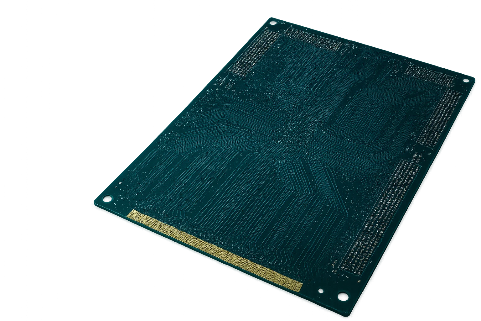
Why Choose Our Backplane PCBs
Engineered for High-Speed, High-Reliability ApplicationsDedicated backplane PCB fabrication addresses the physical constraints of high-layer-count system interconnects, where channel lengths up to 1 meter demand strict suppression of insertion loss, impedance discontinuities, and thermal warpage.
Critical Risk: misaligned lamination and uncontrolled z-axis expansion can compromise high-speed channels in large panels.
Our Solution: zone-controlled lamination, ±25 µm registration accuracy, and resin-reinforced cores maintain stackup stability across 600 mm panels. For channel design tactics and crosstalk control, see our signal integrity guide, or explore High-Speed PCB options when your backplane interfaces directly with high-speed daughtercards.
- Up to 64 layers for complex routing
- Registration accuracy within ±25 µm
- Void-free lamination, less than 0.1%
- Support for 25+ Gbps signal channels
🚀 Quick Quote Request
📋 Get Full Capabilities
Backplane PCB Manufacturing Excellence
Precision Processes and Controlled ReliabilityManufacturing includes mechanical drilling with aspect ratios up to 30:1, precision back-drilling to eliminate stubs above 10 GHz, and controlled lamination cycles. Copper plating thickness variation remains within ±10% for impedance consistency across long traces. Learn how we push drill capability while protecting reliability in our note on aspect ratio drilling.
- Aspect ratio drilling up to 30:1
- Back-drilling for resonance suppression above 10 GHz
- Copper plating variation within ±10%
- Void content less than 0.1%
Backplane PCB Technical Specifications
Performance metrics for high-layer-count and large-format PCBs
| Parameter | Standard Capability | Advanced Capability | Standard |
|---|---|---|---|
Layer Count | 16–32 layers | Up to 64 layers | IPC-2221 |
Panel Size | Up to 500 × 600 mm | Up to 600 × 800 mm | Manufacturing capacity |
Board Thickness | 3.2–6.0 mm | Up to 12 mm | IPC-A-600 |
Impedance Control | ±7% | ±3% single-ended; ±5% differential | IPC-2141 |
Drilling | Mechanical down to 0.25 mm (250 μm) | Laser and back-drilling, aspect ratio up to 30:1 | IPC-2222 |
Surface Finish | HASL Lead-Free, OSP, ENIG | ENEPIG, Immersion Silver, Hard Gold | IPC-4552 |
Certifications | ISO 9001, UL, RoHS | AS9100D, IATF 16949, MIL-PRF-55110 | Industry standards |
Need capabilities beyond this product? Explore our full manufacturing capabilities
Ready to start your PCB project?
Whether you need simple prototypes or complex production runs, our advanced manufacturing capabilities ensure excellent quality and reliability. Get your quote within 30 minutes.
Design Considerations for Backplane PCBs
Designers must account for crosstalk, insertion loss, and skew at 25+ Gbps. Tight dielectric control and symmetrical stackups help maintain impedance within ±3%. When channels approach the limits of FR-4, consider a hybrid stackup using low-loss materials—see related Rogers PCB options for critical layers.
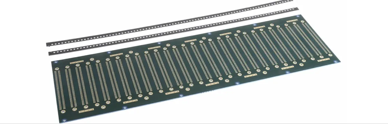
Signal Integrity in High-Speed Backplanes
We validate dielectric constants (Dk) and dissipation factors (Df) across frequency ranges. Low-loss laminates achieve Df less than 0.003. Time-domain reflectometry (TDR) and vector network analyzer (VNA) confirm impedance within ±3%. For routing rules, channel modeling, and reference coupon strategy, see our high-frequency signal integrity checklist.
Quality and Reliability Standards
Backplane production complies with IPC Class 3, AS9100D, and MIL-PRF-55110 standards. Additional certifications include IATF 16949 for automotive and ISO 13485 for medical device backplanes. For workmanship acceptance and audit readiness, review our note on IPC Class 3 compliance.
Industry Applications for Backplane PCBs
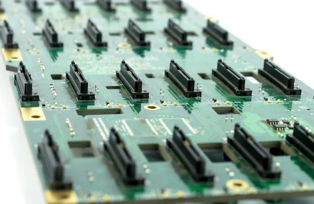
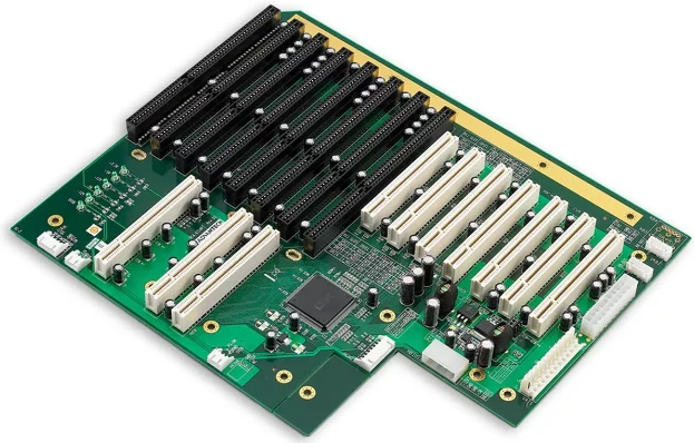
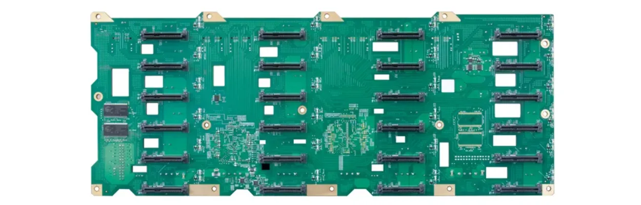
Backplanes power telecom switches, data center fabrics, aerospace avionics, military command systems, and HPC clusters. Where line card densities and connector transitions drive loss budgets, pair the backplane with compliant daughtercards—see High-Speed PCB for complementary designs.
Engineering Assurance & Certifications
Programs are engineered for high-speed reliability with a transparent evidence chain across design, manufacturing, and validation.
Experience: zone-controlled lamination and registration within ±25 µm.
Expertise: TDR/VNA correlation to keep impedance within ±3% and insertion loss targets on track for 25+ Gbps channels.
Authoritativeness: production aligns with IPC Class 3, AS9100D, and IATF 16949; documentation and audits are supported end-to-end.
Trustworthiness: MES links supplier lots and serialization to in-line test data; results include 100% electrical testing and BER less than 10⁻¹² (one error per trillion bits). For drill strategy and stub removal evidence, see aspect ratio drilling.
Frequently Asked Questions
Why is back-drilling important in high-speed backplanes?
What certifications support your backplane PCBs?
How do you ensure material stability for high-speed designs?
Which industries benefit most from your backplane PCBs?
What defines a high-reliability backplane PCB architecture?
Experience Advanced PCB Manufacturing Excellence
From simple prototypes to complex production runs, our world-class factory delivers superior quality, fast turnaround and competitive pricing. Join thousands of satisfied customers who trust us with their PCB manufacturing needs.