
HDI PCB Manufacturer & Fabrication | Quick-Turn Microvia Boards
Factory-direct HDI PCB manufacturer specializing in precision laser microvias and high-volume HDI printed circuit board fabrication. We deliver 1+N+1 to Any-Layer ELIC build-ups, VIPPO copper fill, and fine-pitch BGA escape routing with 24-hour prototype turnaround and scalable volume pricing.
Capabilities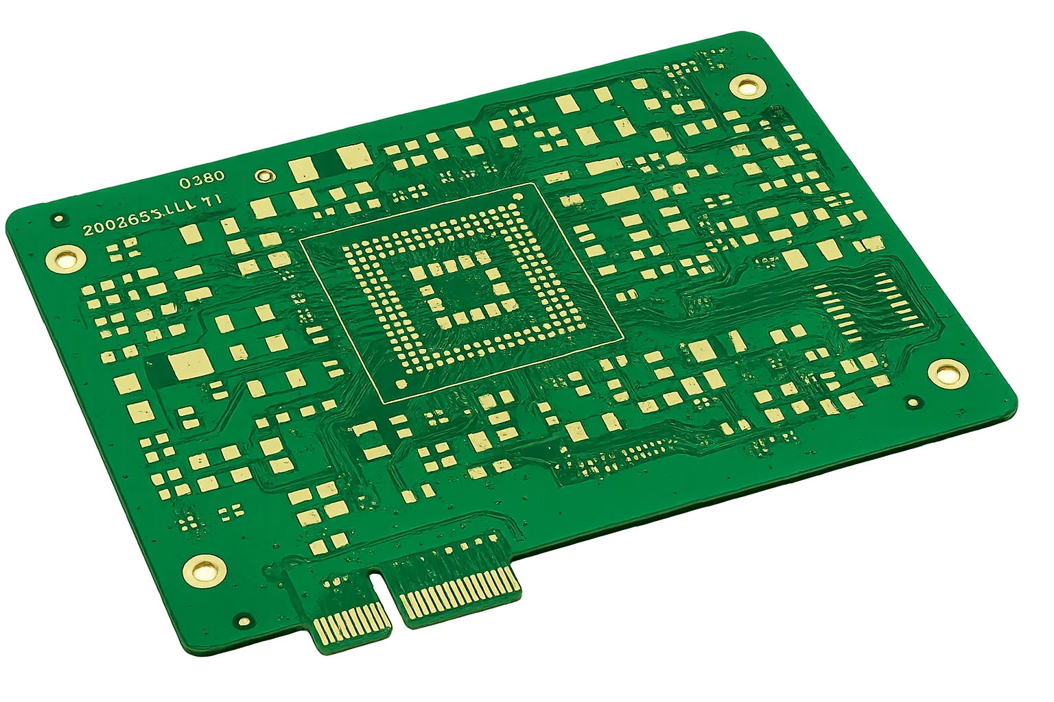
Leading HDI PCB Manufacturer for Density-Driven Designs
Choose HILPCB for rapid-turn microvias, advanced HDI circuit boards, and cost-effective volume productionAs an experienced HDI PCB manufacturer, HILPCB provides the advanced interconnect technologies required when standard through-hole multilayers cannot accommodate fine-pitch component escape, ultra-dense routing, or miniaturized form factors. From smart devices and IoT modules to automotive ADAS and medical electronics, our factory specializes in precision HDI printed circuit boards featuring laser microvias, blind/buried vias, and via-in-pad (VIPPO) architectures.
Our direct manufacturing model eliminates broker markups while delivering rapid 24-hour engineering turnaround for high-density HDI PCBs and seamless scaling into volume production. Whether evaluating standard PCB HDI build-ups or complex multi-layer microvias, our engineering team optimizes panelization to maximize yield and minimize unit cost. If your design requires standard through-hole construction, explore our multilayer PCB capabilities. For loss-critical digital channels, review our high-speed PCB solutions.
What to send for an instant HDI quote: Gerber X2 or ODB++ data, drill files, target stackup, BGA pitch details, impedance requirements, microvia preference (1+N+1, 2+N+2, or Any-Layer), material grade, and volume schedule. Our DFM engineering team evaluates every submission within 2 hours to confirm manufacturability and cost efficiency.
- Factory-direct HDI PCB fabrication with prototype turnaround from 24 hours
- Supported architectures: 1+N+1, 2+N+2, 3+N+3, stacked/staggered, and Any-Layer ELIC
- Laser microvias down to 50 μm (2 mil) with precise copper fill and planarization
- VIPPO via-in-pad technology for seamless 0.4 mm and 0.5 mm BGA fanout
- 100% electrical test, 3D AOI, and X-ray inspection for high-reliability HDI boards
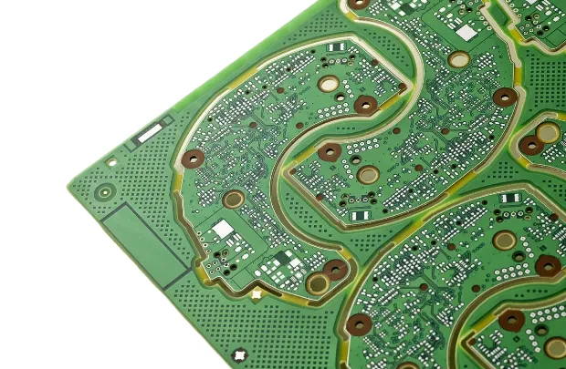
🚀 Quick Quote Request
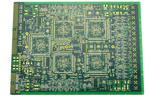
📋 Get Full Capabilities
Precision HDI PCB Fabrication & Sequential Build-Up Excellence
State-of-the-art UV/CO2 laser drilling, copper plating, and VIPPO planarization under tight SPC controlThe reliability of an HDI board depends entirely on rigorous sequential lamination and laser microvia formation. At HILPCB, our manufacturing lines produce advanced HDI circuit boards and custom HDI printed circuit boards using high-precision UV and CO2 laser drilling systems to create clean microvia barrels with controlled taper and zero dielectric damage. Every microvia undergoes chemical desmear and pulse reverse electroplating to achieve solid copper fill with dimple depths controlled under 5 μm.
To ensure seamless downstream assembly, our VIPPO process includes proprietary resin plugging, thermal curing, and ceramic brush planarization before copper capping. For programs transitioning from board fabrication to assembly, combine your order with our PCB assembly or turnkey assembly services for single-source accountability and reduced total cycle time.
- Stacked versus staggered microvia optimization for maximum thermal-shock life
- Automated optical inspection (AOI) and X-ray layer-to-layer registration verification (±15 μm)
- VIPPO planarization with pad co-planarity held within tight SMT mounting tolerances
- High-speed differential impedance control (±5%) correlated via on-panel TDR coupons
- Full material traceability from raw laminate to final microsection test report
HDI PCB Capability & Performance Matrix
Capabilities for density-driven microvia and fine-pitch BGA builds
| Parameter | Standard Capability | Advanced Capability | Standard |
|---|---|---|---|
Layer Count | 4–30 layers | Up to 60+ layers (any-layer) | IPC-2226 |
Base Materials | High-Tg FR-4, low-Dk/Df materials | Megtron 6/7, Isola I-Speed, Rogers RO4000 | IPC-4101 |
Board Thickness | 0.4–3.2 mm | 0.2–6.0 mm | IPC-A-600 |
Min Trace/Space | 75/75 μm (3/3 mil) | 50/50 μm (2/2 mil) | IPC-2221 |
Min Hole Size (Laser) | 0.10 mm (4 mil) | 0.05 mm (2 mil) | IPC-2226 |
Via Technology | Blind/Buried, Microvias (1+N+1, 2+N+2) | Stacked/Staggered, VIPPO, Any-Layer | IPC-6012 |
Aspect Ratio (Microvia) | 0.8:1 | 1:1 | IPC-2226 |
Max Panel Size | 500 × 400 mm | 600 × 500 mm | Manufacturing capability |
Impedance Control | ±10% | ±5% with TDR | IPC-2141 |
Surface Finish | HASL, ENIG, OSP, Immersion Silver | ENEPIG, Soft/Hard Gold, Selective OSP | IPC-4552/4556 |
Quality Testing | E-test, AOI, X-ray | 4-wire Kelvin, Cross-section, IST, HAST | IPC-9252 |
Certifications | ISO 9001, UL, RoHS | IATF 16949, ISO 13485, AS9100, MIL-PRF-31032 | Industry standards |
Lead Time | 7–15 days | 24-hour prototype quick-turn | Production schedule |
Ready to start your PCB project?
Whether you need simple prototypes or complex production runs, our advanced manufacturing capabilities ensure excellent quality and reliability. Get your quote within 30 minutes.
At a Glance: When to Partner with an HDI PCB Manufacturer
Choose HDI when density, package escape, or microvia structure is the main reason the board is difficult. Do not use it as a catch-all for any complex PCB.
- Good fit: fine-pitch BGA escape, VIPPO, blind/buried vias, stacked or staggered microvias, dense routing on high-density interconnect boards and HDI PCBs
- Not the best fit: ordinary 4-12 layer boards with through-hole vias, simple FR-4 boards, or pure high-speed material decisions
- Quote inputs: Gerber/ODB++, drill, PCB HDI stackup, BGA map, impedance targets, material preference, reliability class
- Adjacent pages: multilayer PCB, high-speed PCB, IC substrate PCB
Choose HDI vs Multilayer, High-Speed, and IC Substrate
- HDI PCB: use when microvia build-up, VIPPO, and fine-pitch BGA package escape drive the design.
- Multilayer PCB: use when the board needs more planes and routing layers but can stay with standard through-hole via structures.
- High-Speed PCB: use when channel loss, impedance, or protocol performance is the main driver.
- IC Substrate PCB: use when package-substrate density, SAP/mSAP style features, or semiconductor package escape is the real requirement.
Multilayer HDI PCB Manufacturer Selection: Cost, Prototyping and Build-Up Choice
Choosing between an ordinary multilayer board and an HDI build is a cost decision as much as a technical one. A multilayer HDI PCB manufacturer should be able to show where the crossover lies for your design, because adding build-up layers is expensive and sometimes unnecessary.
When HDI is genuinely required. HDI earns its cost when escape routing from high-pin-count devices cannot be completed in the available layers, when device pitch forces via-in-pad, or when the board outline constrains layer count. When the only driver is a desire for a smaller board, a standard multilayer build with finer design rules may be cheaper and faster.
Cost-effective and low-cost route planning. A cost-effective HDI build usually means minimising the number of sequential laminations, using the largest microvia that still meets density, and avoiding via stacking where staggering is acceptable. When comparing low-cost HDI quotes, compare total cost rather than unit price: a build that reaches volume yield sooner is cheaper than a nominally lower quote that requires several respins.
Advanced via management and prototyping. Via management on an advanced HDI board — deciding which vias are filled, which are stacked, and where backdrilling is needed — is best done with the fabricator before artwork release. An HDI prototype run proves the stackup, the fill quality and the impedance targets on real panels. Prototype results then become the baseline for production acceptance, which is far more reliable than transferring assumptions between suppliers.
If the design is density-driven but not impedance-critical, compare IC substrate options or request an engineering review of the layer budget before committing to a build-up structure.
Where a build-up stack removes the last rigid constraint and the assembly must still fold into a housing, the remaining decision is between HDI on a rigid board and flexible PCB construction; flex keeps the interconnect in the same part rather than adding a connector pair.
For three-dimensional packaging, rigid-flex PCB combines HDI-class microvia density on the rigid sections with a flexible interconnect, which is often cheaper than two HDI boards joined by a cable.
HDI Circuit Board Stack-Up Architecture & Microvia Design
Progression from 1+N+1 to 2+N+2 typically occurs when 0.8 mm pitch BGAs exceed 400–600 pins. In HDI circuit boards, we model via-stub resonance around 0.25λ (one quarter wavelength) near 10 GHz and move critical nets to blind/back-drilled paths. Low-loss transitions (Df 0.009–0.012) are justified once insertion-loss budget falls below ~0.8–1.0 dB/in. See HDI manufacturing and blind via optimization.
Stacked-microvia reliability hinges on uniform copper through sequential plating. We target ≥18–20 μm at the barrel, verified by cross-section. Staggered stacks improve thermal-cycle life by 20–30% but require more area. VIPPO fill CTE is tuned (≈45–55 ppm/°C) to limit solder-joint stress; copper fill is selected when per-via heat dissipation exceeds ~2 W.
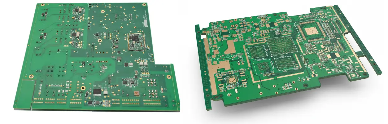
HDI Microvia Technology: Laser Drilling, Via Filling and Blind Buried Structures
HDI microvia technology is defined by three capabilities: forming very small holes reliably, filling and plating them without voids, and stacking or staggering them across multiple build-up layers. Each capability has its own process window, and the design must live inside that window to be manufacturable at volume.
Laser microvia formation. HDI laser microvia drilling uses UV or CO₂ sources depending on dielectric and target diameter. UV lasers produce cleaner sidewalls and tighter diameter control in thin dielectrics; CO₂ is faster where the dielectric suits it. The practical limit is set by the dielectric thickness and the target capture pad, not by the laser alone — a microvia smaller than the process can reliably capture is a yield problem, not a density win.
Via filling and reliability. Via filling (copper-filled or resin-plugged with copper cap) protects stacked vias from entrapped chemistry and mechanical failure. Filled and planarised vias are what allow a subsequent microvia to land directly on top. Incomplete fill shows up later as outgassing, cracked barrels or delamination during assembly reflow, so fill quality is a reliability requirement rather than a cosmetic one.
Blind, buried and stacked structures. An advanced HDI board with blind and buried vias combines microvias with conventional blind and buried through-vias to free routing space in the inner layers. Sequential lamination count rises with each build-up layer, and each additional lamination cycle adds cost, lead time and risk. Where a design only needs one build-up layer, a 1+N+1 structure is almost always the better commercial decision than an any-layer stack.
Stackup and impedance interaction. Microvia stackup choices determine the reference planes available to high-speed signals, so via transitions affect impedance continuity. Review high-speed PCB guidance when HDI is used for density rather than for RF performance.
HDI PCB Fabrication Flow and Inspection Gates
Flow: stackup review -> laser drilling -> desmear/seed -> copper fill or plating -> planarization -> sequential lamination -> imaging/etch -> solder mask/finish -> inspection and electrical test. The key review points are via aspect ratio, capture-pad design, stacked-via count, material movement, impedance plan, and whether any-layer PCB HDI fabrication is justified.
If the density can be solved with a standard multilayer stackup, that is usually the cleaner path. If the density is beyond standard HDI PCB limits, the discussion should move toward IC substrate or package-level design support.
Controlled Impedance in High-Density HDI Printed Circuit Boards
Reduced via stubs and tight plane coupling improve return loss on high-density HDI printed circuit boards and multi-layer HDI PCBs. For >10 Gbps differential pairs, we use blind/back-drilled architectures to eliminate resonant stubs. Material selection turns to ultra-low-loss (Df 0.005–0.007) when the dB/in-GHz product approaches limits. Our impedance modeling uses 3D EM for via arrays and transitions, achieving ±5% production tolerance with coupon correlation. Low-profile copper (Rz <2 μm) reduces conductor loss by 15–20%. Thin build-up dielectrics (50–75 μm) enable PDN loop inductance under 100 pH.
When the high-speed channel also has to hold a loss target at RF or millimetre-wave frequencies, the dielectric matters as much as the via structure; Rogers laminate families provide the Dk/Df stability that microvia transitions alone cannot deliver.
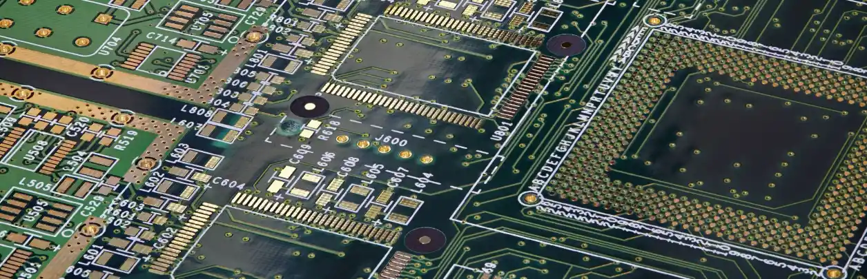
Quality Gates & Reliability Testing for HDI Boards
HDI quality control focuses on registration, via fill, plating continuity, dielectric integrity, and electrical continuity. Depending on the program risk, validation may include AOI, X-ray alignment review, cross-sections, impedance test, and IST planning. Microvia reliability depends on the final stackup and stress profile, so the acceptance plan should be set before release.
Industry Applications for Custom HDI PCB Fabrication
Automotive ADAS: 2+N+2 with selective low-loss RF layers, insertion loss <0.3 dB/in at 77 GHz, copper-filled thermal vias delivering θJB <2 °C/W.
Medical: any-layer miniaturization with ISO 13485 documentation.
Datacom/5G: 25–56 Gbps SERDES; see 5G PCB technology.
Consumer: selective HDI only where density demands, cutting cost by 15–25%.
Engineering Assurance & Certifications as an HDI PCB Manufacturer
Experience: production-proven 1+N+1 to any-layer programs with zone-controlled lamination and LDI registration.
Expertise: TDR/VNA for via transition models; SPC on plating and drill registration; Cpk targets ≥1.33.
Authoritativeness: IPC Class 3, IATF 16949, ISO 13485, AS9100; audits and documentation end-to-end.
Trustworthiness: MES tracks lot codes and serialization to in-line test data; IST/HAST reports available for qualification.
- Process controls: plating thickness, lamination pressure/temperature, laser energy
- Traceability: unit serialization, component lot tracking, digital traveler
- Validation: IST, HAST, microsection reviews, impedance coupons
Frequently Asked Questions
Why choose HILPCB as your HDI PCB manufacturer?
How do I choose between 1+N+1, 2+N+2, and Any-Layer HDI PCB fabrication?
What are the minimum laser microvia diameter and aspect ratio capabilities?
How does VIPPO (Via-in-Pad Plated Over) improve HDI printed circuit board assembly?
What design factors most influence HDI PCB manufacturing cost and lead time?
Can HILPCB guarantee tight controlled impedance on high-speed HDI boards?
What files and documentation are required for a buildable HDI PCB quote?
What is HDI microvia technology?
Experience Advanced PCB Manufacturing Excellence
From simple prototypes to complex production runs, our world-class factory delivers superior quality, fast turnaround and competitive pricing. Join thousands of satisfied customers who trust us with their PCB manufacturing needs.