
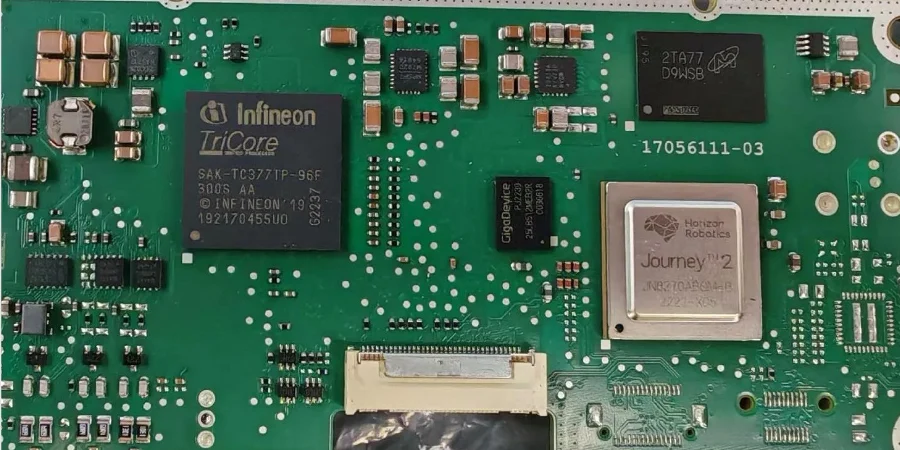
An ADAS radar PCB operating at 77–81 GHz is not a conventional automotive board with tighter tolerances — it is a millimeter-wave RF component where the dielectric, copper foil, and etch accuracy directly determine antenna pattern, detection range, and angular resolution. Selecting a manufacturer for this board requires verifying specific RF process capabilities, material control evidence, and automotive quality documentation — not just reading a capability list.
This guide helps hardware engineers, quality/NPI teams, and procurement buyers make three decisions: which laminate and stackup fit the radar application, which process tolerances the manufacturer must hold, and which evidence to request before releasing an RFQ or approving a PPAP.
What Makes 77 GHz ADAS Radar PCB Manufacturing Different From Standard Automotive PCBs?
At 77 GHz, the half-wavelength is approximately 1.95 mm, and a microstrip patch antenna on 5-mil (127 µm) Rogers RO3003 is roughly 1.07 mm wide. A ±25 µm etch tolerance shifts the antenna resonance by approximately ±1.81 GHz. Standard FR-4 (Dk ~4.5, Df ~0.020) is unsuitable because its dielectric loss at 77 GHz would consume the entire link budget over a few millimeters of trace. These physics constraints mean the PCB manufacturer must control dielectric thickness, copper roughness, and trace geometry to tolerances that standard automotive PCB lines cannot hold.
The key differences are:
- Material: Low-loss PTFE or ceramic-filled hydrocarbon laminates (Dk < 3.5, Df < 0.002 at 10 GHz) replace FR-4. Hybrid stackups combine a thin RF core (e.g., RO3003G2) with an FR-4 or low-loss digital sub-stack.
- Copper foil: VLP or HVLP copper (Ra ≤ 0.6 µm) is required because standard ED copper (Ra ~2.0 µm) increases conductor loss by 30–50% at 77 GHz.
- Etch tolerance: Line-width control of ±10 µm or better is needed for antenna and RF trace consistency; registration accuracy of ±25 µm is expected.
- Surface finish: Solder mask over mmWave transmission lines adds 0.1–0.2 dB/cm loss; ENEPIG or OSP is preferred over ENIG on RF paths due to nickel absorption.
- Reliability: Automotive qualification requires 1,000–2,000 thermal cycles from -40 °C to +125 °C (AEC-Q100 Grade 1) or +150 °C (Grade 0), plus THB/HAST, vibration, and salt spray testing.
How Do You Select the Right Laminate for Your ADAS Radar Application?
Material selection depends on the radar type, frequency band, and whether FR-4 can appear in the stackup at all. The following matrix maps common ADAS radar applications to laminate families and FR-4 eligibility.
ADAS Radar PCB Material Selection Matrix
| Radar Application | Typical Band | Recommended RF Laminate | FR-4 in Stackup? | Key Material Risk |
|---|---|---|---|---|
| Long-range front radar | 76–81 GHz | RO3003G2 (Dk 3.0, Df 0.0013) | No (digital sub-stack only) | Dk drift shifts antenna resonance; Df increase reduces detection range |
| 4D imaging radar | 77–81 GHz | RO3003G2 or TSM-DS3 | No | Multi-channel phase consistency requires Dk CPK ≥ 1.33 |
| Corner / short-range radar | 77–81 GHz | RO4835 or Megtron 6 | Conditional (low-loss prepreg only) | Lower loss budget tolerance; hybrid bondply compatibility |
| 24 GHz legacy radar | 24 GHz | RO4350B | Yes (standard FR-4 prepreg acceptable) | Phase-out risk; long-term laminate availability |
A 4–6 layer stackup is typical for 77 GHz modules: a thin RF core (127–254 µm) carries the antenna and RF traces, while the digital sub-stack handles power, control, and baseband signals. Hybrid lamination is challenging because PTFE-based laminates cure at 370–400 °C while FR-4 cures at 180–200 °C, requiring sequential lamination and a controlled cooling rate of ≤ 2 °C/minute to prevent warpage and via cracking.
Which Process Tolerances Must the Manufacturer Control for 77 GHz Radar PCBs?
The following parameter-risk table maps each manufacturing tolerance to its radar performance impact. This is the evidence buyers should request and engineers should verify during DFM review.
Parameter-Risk-Evidence Matrix for 77 GHz ADAS Radar PCBs
| Parameter | Required Tolerance | Radar Impact if Out of Spec | Evidence to Request |
|---|---|---|---|
| Dielectric constant (Dk) | ±0.04 process, CPK ≥ 1.33 | Antenna resonance shift; beam-steering error | COA per lot; Dk coupon test at 10 GHz |
| Dk thermal drift | ≤ 0.21% across -40 to +125 °C | Frequency shift over temperature; calibration invalidation | Laminate datasheet; thermal chamber Dk measurement |
| Loss tangent (Df) | < 0.002 at 10 GHz | Insertion loss increase; detection range reduction | COA; S-parameter coupon report |
| Copper foil roughness (Ra) | ≤ 0.6 µm (HVLP/VLP) | Conductor loss +30–50% vs HVLP; range degradation | Foil type on stackup drawing; supplier confirmation |
| Line width / etch tolerance | ±10 µm (±0.4 mil) | ±25 µm shift → ±1.81 GHz resonance shift | LDI capability; etch coupon measurement; AOI data |
| Registration accuracy | ±25 µm | Layer misalignment; impedance discontinuity; via open | X-ray registration report; CCD alignment capability |
| Impedance control | 50 Ω / 100 Ω ±5% | Return loss; EVM degradation; ACLR failure | TDR coupon report per panel; SPC chart |
| Dielectric thickness (RF layer) | ±10% | Impedance shift; antenna gain variation | Cross-section measurement; lamination press profile |
| Plated via integrity | IPC Class 3; ≥ 25 µm barrel copper | Via cracks after ~200 thermal cycles; field failure | Cross-section; thermal cycling test report; CAF data |
What Automotive Reliability Gates Must ADAS Radar PCBs Pass?
ADAS radar PCBs are typically classified at ASIL-B or higher under ISO 26262, and the PCB itself is treated as a critical passive component under the AEC-Q100/Q200 zero-defect philosophy. The manufacturer must demonstrate a quality management system registered to IATF 16949, not just ISO 9001.
The core reliability tests and their pass criteria are:
- Thermal shock / cycling: 1,000–2,000 cycles between -40 °C and +125 °C (Grade 1) or +150 °C (Grade 0). No via cracking, delamination, or solder joint fatigue.
- Temperature Humidity Bias (THB/HAST): 85 °C / 85% RH with applied voltage for 1,000 hours. Evaluates anti-CAF capability and insulation resistance.
- Vibration and mechanical shock: Simulates vehicle road conditions. Verifies structural integrity and solder joint strength.
- Salt spray: 96+ hours. Verifies surface finish and solder mask corrosion resistance.
These tests must be documented through APQP and PPAP. The PPAP package (typically Level 3 for automotive) includes design records, PFMEA, control plan, MSA, initial process capability studies (Cpk > 1.67), material certifications, and full-dimensional measurement reports. The control plan must specify 100% TDR testing or SPC sampling for RF trace impedance, and the manufacturer must maintain board-level traceability via QR code linking to raw material lot, equipment, operator, and test data.
How Do You Select an ADAS Radar PCB Manufacturer?
Use the following supplier selection matrix to score candidates. Each criterion has a pass/fail threshold and evidence requirement. A manufacturer that cannot provide the evidence should not be approved for 77 GHz radar PCB production, regardless of price or lead time.
ADAS Radar PCB Supplier Selection Scorecard
| Criterion | Pass Threshold | Evidence Required |
|---|---|---|
| RF material processing | PTFE/ceramic-filled laminate experience; plasma desmear (CF₄/O₂) | Process flow; plasma equipment spec; prior RO3003/RO4835 build records |
| Etch / imaging capability | LDI; ±10 µm line-width control | LDI equipment list; etch coupon data from prior 77 GHz builds |
| Hybrid lamination | Sequential lamination; cooling rate ≤ 2 °C/min | Press profile; cross-section of prior hybrid stackup |
| Impedance control | ±5% with TDR verification | TDR coupon report; SPC chart; impedance simulation capability |
| Quality system | IATF 16949; IPC Class 3; ISO 26262 awareness | Certificate number and scope; audit report; APQP/PFMEA examples |
| Reliability testing | 1,000+ thermal cycles; THB 85/85 1000 h; CAF data | Test report with sample size, conditions, and pass criteria |
| PPAP capability | PPAP Level 3; 18-element package; Cpk > 1.67 | Prior PPAP submission sample; control plan template |
| Traceability | Board-level QR code; MES-linked process data | Traceability system demo; recall procedure |
What Should an ADAS Radar PCB RFQ Include?
A complete RFQ for an ADAS radar PCB must specify not only the board geometry but also the material, process, and evidence requirements that determine whether the manufacturer can meet automotive reliability targets. Use this checklist before sending the RFQ.
Design data to submit:
- Gerber/ODB++ files with impedance-controlled net list
- Stackup drawing specifying RF laminate grade, Dk/Df targets, copper foil type (HVLP/VLP), and dielectric thickness per layer
- Antenna array layout with reference plane and keepout zones
- Drill table with via types (through, blind, buried, resin-plugged) and tolerances
- Surface finish specification (ENEPIG or OSP preferred for RF paths; no solder mask over mmWave traces)
- Panelization and fiducial requirements
Process and evidence to request:
- LDI imaging confirmation and etch tolerance capability (±10 µm target)
- Hybrid lamination press profile and cooling rate (≤ 2 °C/min)
- TDR impedance coupon plan (100% per panel or SPC sampling)
- Plasma desmear process for PTFE surfaces (CF₄/O₂)
- Thermal cycling test plan (1,000+ cycles, -40 to +125 °C)
- THB/HAST and CAF test data
- PPAP Level 3 package with control plan, PFMEA, MSA, and Cpk data
- Material COA per lot with Dk/Df measurement at 10 GHz
- Board-level traceability system description
Acceptance criteria to define:
- IPC Class 3 for plated vias and annular rings
- Impedance: 50 Ω / 100 Ω ±5% verified by TDR coupon
- No delamination, via cracking, or impedance failure after thermal cycling
- AOI and AVI 100% coverage on inner and outer layers
- Electrical test 100% against netlist
What NPI Quality Gates Apply From EVT Through SOP?
Automotive-grade ADAS radar PCB programs follow a staged NPI process. Each stage closes a different risk before the program scales to mass production.
NPI Quality Gates: From Prototype to SOP
Each stage closes a different risk before the program scales
Objective: Verify design functionality and RF performance. Flying probe test acceptable. Material substitution allowed if Dk/Df is equivalent. Freeze critical RF nets and antenna layout.
Objective: Safety and environmental reliability testing. Submit PPAP Level 3. Lock laminate grade, stackup, and surface finish. TDR coupons required on every panel.
Objective: Verify Run@Rate capacity. Monitor first pass yield through Early Production Containment (EPC). Confirm tooling, fixtures, and SPC stability.
Objective: Continuous improvement via SPC and 8D. Maintain Cpk > 1.67 on critical parameters. Full traceability from material lot to shipped board.
Common Questions
Why is ADAS radar PCB manufacturing more demanding than standard automotive PCB production?
At 77 GHz, the PCB is part of the antenna system. Dielectric constant, copper roughness, and etch tolerance directly determine antenna resonance, beam pattern, and detection range. Standard automotive PCB lines typically cannot hold ±10 µm etch tolerance or process PTFE-based laminates with plasma desmear, which are mandatory for 77 GHz boards.
Which material should I choose for a 77 GHz front radar?
RO3003G2 (Dk 3.0, Df 0.0013 at 10 GHz) is the most common choice for long-range front radar. It offers low Dk thermal drift (0.21% across -40 to +125 °C) and stable z-axis CTE (~24 ppm/°C). FR-4 is not acceptable in the RF layers; it may appear only in the digital sub-stack of a hybrid build, bonded with a compatible low-loss prepreg.
What evidence should I request from the manufacturer before approving PPAP?
Request: material COA with Dk/Df measurement at 10 GHz per lot, TDR impedance coupon report, thermal cycling test report (1,000+ cycles, -40 to +125 °C), THB/HAST and CAF data, cross-section showing via plating (≥ 25 µm barrel copper per IPC Class 3), control plan with SPC charts, PFMEA, MSA, and initial Cpk data (> 1.67 on critical parameters).
Can I use ENIG surface finish on 77 GHz RF traces?
ENIG is generally not recommended on RF paths at 77 GHz because the nickel layer introduces absorption loss. ENEPIG or OSP is preferred. Solder mask should not cover mmWave transmission lines because it adds 0.1–0.2 dB/cm loss.
What is the difference between AEC-Q100 Grade 0 and Grade 1 for radar PCBs?
Grade 1 covers -40 °C to +125 °C, which is sufficient for most ADAS radar modules mounted behind the vehicle grille. Grade 0 covers -40 °C to +150 °C, required for engine-bay or powertrain-adjacent placements. The thermal cycling test count and temperature range must match the target grade.
Conclusion
Selecting a manufacturer for ADAS radar PCB manufacturing at 77 GHz is a procurement and engineering decision that hinges on verifiable RF process capability, not generic automotive PCB experience. The manufacturer must demonstrate PTFE laminate processing, LDI-based etch control at ±10 µm, hybrid lamination with controlled cooling, ±5% impedance verification by TDR, and a full PPAP Level 3 package with IATF 16949 quality system registration.
Use the material selection matrix to match the laminate to the radar application, the parameter-risk-evidence table to specify what the manufacturer must control and prove, and the supplier scorecard to qualify candidates before releasing the RFQ. The manufacturer's responsibility covers bare-board fabrication and process evidence; system-level radar performance validation, ISO 26262 safety case, and vehicle integration remain the OEM's or Tier 1's responsibility.
HILPCB provides high-frequency PCB manufacturing with Rogers, Taconic, and PTFE laminate processing, ±5% impedance control verified by TDR, and turnkey assembly for radar module production. Contact the engineering team to review your stackup and RFQ requirements.