
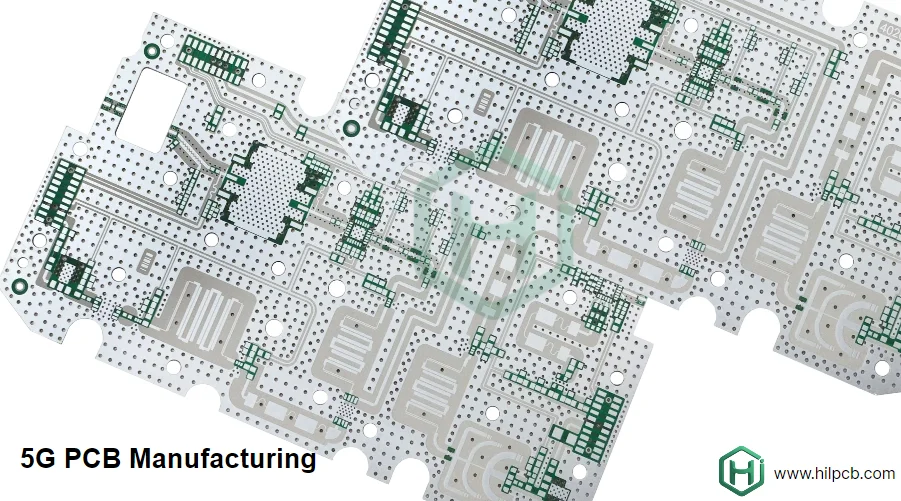
With the rapid deployment of 5G networks and the continuous maturation of 6G research, Massive MIMO (Multiple-Input Multiple-Output) technology has become the core standard for wireless communication. In this architecture, the Beamforming module board acts as a crucial medium connecting RF front-ends, antenna arrays, and baseband processing units. Its design and manufacturing quality directly determine the coverage, capacity, and signal stability of the entire base station. Achieving stringent Beamforming module board compliance is an enormous challenge for both RF hardware engineers and PCB manufacturers.
This article delves into the technical difficulties of beamforming module boards, from material selection and stack-up design to precision manufacturing processes. We aim to provide a comprehensive guide, equivalent to an in-depth Beamforming module board checklist, to help you successfully deliver high-performance communication products, whether for massive base station deployments or data-center Beamforming module board applications requiring ultra-low latency.
The dual challenges of high frequencies and mixed signals
The primary function of a beamforming module is to control the phase and amplitude of signals transmitted by each antenna element, thereby creating highly directional signal beams. This requires the PCB to simultaneously process:
- High-Frequency RF Signals: Operating in Sub-6GHz or even mmWave (millimeter wave) bands (such as 28GHz, 39GHz), these signals are extremely sensitive to transmission loss and phase variations.
- High-Speed Digital Signals: Data interfaces like CPRI/eCPRI, or high-speed data streams connecting to baseband chips, demand strict impedance control and low cross-talk.
- Power and Control Signals: Supplying stable power to numerous power amplifiers (PAs) and low-noise amplifiers (LNAs) while dissipating the massive heat they generate.
These mixed demands make traditional FR-4 materials inadequate. To meet Beamforming module board compliance, a hybrid stack-up (Hybrid Stack-up) design has become the industry standard.
Hybrid Stack-up: The perfect balance of cost and performance
High-frequency signals require materials with low Dielectric Constant (Dk) and low Dissipation Factor (Df), such as PTFE (Polytetrafluoroethylene) or hydrocarbon resin-based materials like the Rogers 4000 series. However, utilizing these high-performance materials for all layers is prohibitively expensive and unnecessary for low-speed digital or power layers.
Therefore, the core strategy for beamforming boards is the Hybrid Stack-up.
- RF Signal Layers: High-frequency materials (e.g., Rogers RO4350B, RO4835) are utilized for the top and bottom layers, or specific inner layers dedicated to RF signal transmission, minimizing insertion loss and ensuring precise phase control.
- Digital/Power/Ground Layers: High-quality FR-4 or High-Tg materials are used for inner layers that process digital signals, power, and ground planes, balancing the overall cost of the board.
A successful hybrid stack-up design requires a deep understanding of material properties. During the lamination process, different materials exhibit varying Coefficients of Thermal Expansion (CTE), which can lead to board warpage, delamination, or via failures. Professional PCB manufacturers, like HILPCB, utilize precise CTE matching and optimized pressing parameters to ensure the reliability of hybrid boards, a critical step often found on any rigorous Beamforming module board checklist.
Precision manufacturing: Defending Signal Integrity (SI)
Material selection is only the first step. For mmWave bands, minor manufacturing deviations can trigger the "butterfly effect," leading to severe signal degradation. Beamforming module board compliance mandates extreme precision in the manufacturing process:
1. Low-roughness copper foils
At high frequencies, the "Skin Effect" forces current to concentrate on the surface of the copper conductor. If the copper surface is rough, the path the current travels lengthens, increasing conductor loss. Standard copper foils cannot meet these requirements. For beamforming boards, especially in the mmWave bands, Very Low Profile (VLP) or Ultra-Low Profile (HVLP) copper foils must be used. Controlling surface roughness (Rz) to within 2μ m or even lower is key to reducing high-frequency insertion loss.
2. Strict impedance control and phase matching
Beamforming relies on precise phase differences. If the impedance of transmission lines fluctuates, it causes signal reflections, subsequently altering the signal phase.
- Etching precision: Etching tolerance for RF traces must typically be controlled within ± 10% or even ± 5%. This requires the use of Laser Direct Imaging (LDI) technology and advanced etching line control systems to ensure straight trace edges and a trapezoidal cross-section close to a perfect rectangle.
- Phase consistency: For differential pairs or multi-channel RF lines, physical lengths and electrical lengths must match strictly to ensure signal arrival at the antenna elements is perfectly synchronized.
3. Backdrilling technology (Backdrill)
In multi-layer boards, vias are used for signal transitions between layers. However, the unused portion of the via (the "stub") acts like an antenna at high frequencies, creating resonance and severely degrading signal quality. Backdrilling mechanically removes these excess stubs. Controlling the backdrill depth with high precision to minimize the remaining stub length (typically required to be less than 10 mils) is critical for improving high-frequency signal integrity.
📡 Core Technology: Taming high-frequency & high-speed physical layers
Addressing signal integrity and thermal challenges in 5G/6G beamforming modules
<div style="display: grid; grid-template-columns: repeat(auto-fit, minmax(300px, 1fr)); gap: 20px;">
    <div style="background: rgba(255,255,255,0.05); border: 1px solid rgba(255,255,255,0.1); border-radius: 12px; padding: 25px;">
        <div style="display: flex; align-items: center; margin-bottom: 15px;">
            <span style="font-size: 1.5em; margin-right: 10px;">📉</span>
            <strong style="color: #7dd3fc; font-size: 1.15em;">Ultra-Low Loss Interconnects</strong>
        </div>
        <p style="color: #cbd5e1; font-size: 0.9em; line-height: 1.6; margin: 0;">Beyond basic material selection (like Rogers 4000 series), the critical factor lies in <strong>copper foil roughness control (HVLP)</strong> and mitigating the skin effect. We strictly control the line etching factor (Etch Factor) to ensure trace cross-sections approach an ideal rectangle, minimizing high-frequency insertion loss.</p>
    </div>

    <div style="background: rgba(255,255,255,0.05); border: 1px solid rgba(255,255,255,0.1); border-radius: 12px; padding: 25px;">
        <div style="display: flex; align-items: center; margin-bottom: 15px;">
            <span style="font-size: 1.5em; margin-right: 10px;">🎯</span>
            <strong style="color: #7dd3fc; font-size: 1.15em;">Precision Phase & Impedance</strong>
        </div>
        <p style="color: #cbd5e1; font-size: 0.9em; line-height: 1.6; margin: 0;">Beamforming relies on accurate phase differences. Through LDI (Laser Direct Imaging) exposure, we achieve a <span class="math-inline">±5%</span> trace width tolerance. Combined with customized Dk extraction models, we ensure impedance and phase consistency across all RF channels.</p>
    </div>

    <div style="background: rgba(255,255,255,0.05); border: 1px solid rgba(255,255,255,0.1); border-radius: 12px; padding: 25px;">
        <div style="display: flex; align-items: center; margin-bottom: 15px;">
            <span style="font-size: 1.5em; margin-right: 10px;">🔥</span>
            <strong style="color: #7dd3fc; font-size: 1.15em;">Advanced Thermal Management</strong>
        </div>
        <p style="color: #cbd5e1; font-size: 0.9em; line-height: 1.6; margin: 0;">High-power PAs generate immense heat. We support <strong>embedded copper coins (Copper Coin)</strong> and ultra-dense thermal via arrays. This establishes a highly efficient Z-axis heat transfer path directly to the system heat sink, preventing thermal derating.</p>
    </div>
</div>

<div style="margin-top: 30px; padding: 20px; background: rgba(56,189,248,0.1); border-radius: 10px; border-left: 4px solid #38bdf8;">
    <strong style="color: #38bdf8; font-size: 1em; display: block; margin-bottom: 8px;">💡 HILPCB High-End Manufacturing Tip:</strong>
    <p style="color: rgba(255, 255, 255, 0.9); font-size: 0.95em; line-height: 1.7; margin: 0;">For 77GHz+ or 112G PAM4 signals, we recommend using <strong>ultra-thin dielectric glass weave (E-Glass/Low Df)</strong> paired with pulse plating processes. We provide quantified outbound microsection reports to ensure your design metrics are perfectly reproduced at the physical layer.</p>
</div>
Hybrid manufacturing yield: Mastering alignment, plating, and lamination
The manufacturing yield of hybrid boards directly impacts project costs and delivery times, especially for projects demanding Beamforming module board quick turn. The core challenge lies in managing the differing physical and chemical properties of the various materials.
- Layer Alignment: Because FR-4 and PTFE materials have different expansion and contraction rates during lamination, independent scaling compensation factors must be applied to different material layers. Advanced X-ray alignment drilling systems are crucial for ensuring high-precision registration.
- Plating Quality: Desmearing and activating PTFE via walls is a prerequisite for successful plating. Inadequate plasma treatment can lead to poor adhesion between the copper layer and the via wall, potentially causing plating separation after thermal shock or long-term use.
- Lamination Parameters: The lamination window (temperature, pressure profiles) must be optimized for the specific stack-up structure. Improper parameters can lead to insufficient resin filling, delamination, or uneven board thickness—all of which are fatal flaws for compliance.
Through standardized operational procedures and a profound understanding of hybrid lamination processes, HILPCB effectively controls these variables, providing customers with highly reliable HDI PCBs and hybrid boards.
📡 HILPCB: High-precision manufacturing solutions for beamforming modules
Deep expertise in phased array radars and 5G/6G base stations, guaranteeing extreme physical layer precision
Supporting the full range of Rogers (3003/4350B), Taconic, and Isola RF substrates. Proficient in multi-layer hybrid lamination processes up to 30 layers. Precise Coefficient of Thermal Expansion (CTE) matching control ensures consistent beam phasing.
Equipped with backdrilling capabilities featuring ±0.05mm depth control precision, maintaining stub lengths consistently under 50μ m. Effectively eliminates high-frequency resonance points, ensuring signal purity for beamforming circuits in 28GHz+ bands.
Relying on precision etching and inline linewidth monitoring, impedance control tolerances are converged to ±5%. Every order is accompanied by a full-channel TDR measurement report, ensuring amplitude and phase consistency of differential pairs and RF feeders fully complies with MSA standards.
As a leading PCB solutions provider, we offer more than just manufacturing; we deeply engage in our customers' SI/PI simulation reviews. Tailored to the high-density characteristics of beamforming, we accelerate your productization process comprehensively, from stack-up optimization to final product delivery.
Reliability testing and verification: Ensuring long-term stable operation
The ultimate measure of Beamforming module board compliance is the product's long-term reliability in actual application environments. This requires verification through a series of rigorous tests.
- Thermal Cycling Test: Simulates scenarios where equipment repeatedly operates under different temperatures to verify the reliability of vias and solder joints, especially in hybrid boards where CTE mismatches are present.
- Damp Heat Test: Evaluates the performance stability of the PCB under high temperature and high humidity conditions, checking for delamination or changes in Dk/Df caused by moisture absorption.
- Peel Strength Test: Verifies the bond strength between traces and substrates, and between different layers, ensuring they will not separate under mechanical or thermal stress.
- Warpage Control: Beamforming modules usually require Surface Mount Technology (SMT) assembly, placing extreme demands on the PCB's flatness. Through symmetrical stack-up design and optimized lamination processes, warpage can be controlled to within 0.75%.
A comprehensive Beamforming module board testing protocol is the final defense in delivering high-quality products, which is especially critical for applications like data-center Beamforming module board that demand 24/7 continuous operation.
Common Questions
Why is a Rogers/PTFE plus FR-4 hybrid stack-up often used in beamforming module boards?
Because the RF layers need low-loss, stable materials while the digital and power sections do not always justify the same cost. A hybrid stack-up keeps premium laminates where phase accuracy and insertion loss matter most and uses FR-4 elsewhere to control budget.
Why do copper roughness and impedance control matter so much in beamforming modules?
At high frequencies, conductor loss and dielectric loss rise quickly, and rough copper adds even more attenuation. Tight impedance control also limits reflections so channel-to-channel amplitude and phase behavior stay more consistent.
Why is backdrilling important on beamforming module boards?
Unused via stubs behave like resonant discontinuities at high frequency. Backdrilling shortens those stubs, reduces reflections, and helps preserve cleaner RF transmission paths.
Which reliability checks matter most before shipment?
Thermal cycling, damp heat, peel-strength, and warpage verification are all critical. Together they confirm that hybrid materials, vias, copper adhesion, and flatness remain stable through assembly and long-term operation.
Conclusion
Achieving Beamforming module board compliance is a complex systems engineering task requiring close collaboration between design engineers and PCB manufacturers. Every step is indispensable, from front-end material selection and stack-up planning to precision process control during manufacturing, down to final reliability verification. Understanding and mastering core elements like Rogers/PTFE and FR-4 hybrid lamination, low-roughness copper foils, backdrilling technology, and precise impedance control are key to successfully developing next-generation 5G/6G communication products.
At HILPCB, we provide not only advanced manufacturing services but also strive to be your technical partner. Whether you are conducting prototype development for a Beamforming module board low volume run or require expedited production for a Beamforming module board quick turn project, our professional engineering team is ready to support you. We recommend sharing a detailed Beamforming module board checklist with us at project kickoff to collaboratively build high-performance PCB products that meet the most stringent compliance requirements. We offer comprehensive services from PCB manufacturing to Turnkey PCBA assembly, ensuring your design is flawlessly realized.