
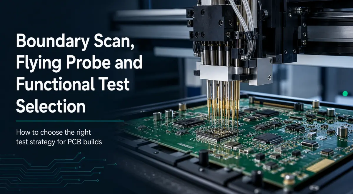
Boundary scan JTAG is a structural test method that controls and observes supported device pins through an IEEE 1149.1 Test Access Port without probing every net physically. On dense 5G and emerging 6G communication boards, it can expose otherwise inaccessible digital interconnect faults, but only where the silicon, BSDL data, board architecture, power state, and test program provide controllability and observability.
Key Takeaways
- IEEE 1149.1 uses TCK, TMS, TDI, and TDO; TRST is optional.
- Coverage belongs to a specific board, BSDL set, fault model, and test program—not merely a JTAG header.
- IEEE 1149.6 can check supported AC-coupled/differential interconnect structure, not eye, BER, loss, or RF performance.
- JTAG may expose covered opens or bridges beneath a BGA, but not void geometry or every solder defect.
- Programming success does not prove boot, interface training, clock quality, or radio performance.
Table of Contents
- What Boundary Scan Can Prove
- Qualify Coverage by Controllability and Observability
- Design a Production-Ready JTAG Chain
- Use a Safe Bring-Up Staircase
- Keep IEEE 1149.6 Separate from RF Validation
- Combine JTAG with the Right Test Methods
- Control Programming Security and Traceability
- Common Failure Modes and First Evidence
- Boundary Scan JTAG RFQ Checklist
- Reference Standards and Responsibility Boundaries
- How HILPCB Can Support the Test Package
- Frequently Asked Questions
What Boundary Scan Can Prove
An IEEE 1149.1 device contains a TAP controller, instruction/data registers, and boundary cells at supported pins. EXTEST drives and samples those pins; BYPASS shortens the path through inactive devices. IDCODE helps identify silicon but is not mandatory in every 1149.1 implementation.
The core TAP signals are TCK, TMS, TDI, and TDO. Optional TRST resets the controller. Compliance pins, reset straps, multiplexed debug pins, or boot modes may also be required and must be reproduced at the production station.
BSDL describes pin mapping, TAP pins, instruction length, register access, boundary cells, compliance patterns, and declared 1149.6 capability. It must match the exact device, package, and revision; a mismatched file can cause false diagnostics or unsafe drive.
Qualify Coverage by Controllability and Observability
Ask which nodes can be driven and observed, in which power/reset state, with which model—not only whether the board has JTAG.
| Circuit object | Coverage precondition | What JTAG may prove | What remains unproven |
|---|---|---|---|
| Two-ended digital net | Compatible cells, safe EXTEST, correct BSDL/netlist | Observable opens, bridges, shorts, stuck states | Timing, jitter, noise margin, stress intermittency |
| One-ended digital net | Far-end fixture I/O or observable cluster behavior | Partial connectivity/logic response | Complete open coverage without another endpoint |
| Non-JTAG memory/logic | Required bus, clock, reset, and response nodes accessible | Selected reads, writes, functions, connections | Internal nodes, full function, rated speed |
| BGA/LGA joint | Relevant ball has a usable cell and observable net | Electrical open/bridge symptom | Voids, head-in-pillow, strength, uncovered balls |
| AC-coupled differential link | 1149.6 support at required endpoints and valid model | Supported structural open/short conditions | Eye, BER, loss, skew, return loss |
| RF path | Only control/status pins are normally accessible | Control connectivity and selected states | Gain, noise, phase, harmonics, S-parameters |
| Power network | Safe states plus accessible enable/status nodes | Selected enable/reset/power-good logic | Impedance, ripple, stability, transient response |
| Programmable target | Supported algorithm, accessible signals, authorized security state | Program/verify/erase/read as supported | Boot, application behavior, system security |
A defensible report identifies the released design/model set, counts covered pins or nets by fault class, and lists exclusions. A percentage without denominator and fault model is not evidence.
Build a Coverage Qualification Package
Coverage changes when a silicon revision, assembly option, BSDL, netlist, or test algorithm changes. Release these identities together instead of treating the executable as a self-contained test.
| Qualification item | Minimum controlled content | Why it matters |
|---|---|---|
| Board identity | PCB and PCBA part number, revision, BOM option, netlist hash | Prevents a valid test from being applied to the wrong wiring or population |
| Device identity | Manufacturer part, package, silicon revision, IDCODE expectation where implemented | Connects the physical assembly to the correct boundary architecture |
| BSDL set | Vendor source, file/version/date, syntax status, hash, approved deviations | Makes model changes visible and repeatable |
| Chain model | Connector pinout, TDI-to-TDO order, IR lengths, optional-device bypass | Defines what the station must detect before interconnect vectors run |
| Operating state | Rail sequence, TAP voltage, reset/boot/compliance patterns, clocks, watchdog handling | Establishes the conditions under which results are meaningful |
| Drive-safety file | Contention exclusions, protected outputs, unpowered domains, maximum test frequency | Prevents test vectors from damaging hardware or creating false failures |
| Coverage statement | Fault classes, covered and excluded nets/pins, cluster assumptions, 1149.6 endpoints | Explains exactly what a pass does and does not claim |
| Production evidence | Controller/adapter/fixture, software and test versions, limits, serial result schema | Allows a failure, retest, or later audit to be reproduced |
Requalify affected coverage when any controlled identity changes. A replacement component may be functionally equivalent yet expose different cells, instructions, compliance patterns, or safe-state behavior.
Design a Production-Ready JTAG Chain
Complete JTAG DFT before layout release; a late connector cannot repair missing support, unsafe states, voltage-domain errors, or an open optional-device path.
Use this design checklist:
- Inventory devices. Record exact part/package/revision, supported instructions, IR length, IDCODE if present, and vendor BSDL.
- Validate BSDL. Check syntax/semantics and schematic pins; release the approved file name, version, date, and hash.
- Define chain order. Document connector, every device, and final TDO; expose useful TDO-to-TDI boundaries for segmentation.
- Bypass options. An absent device or daughtercard must not open the chain.
- Manage voltage domains. Verify controller voltage, thresholds, translation, sequence, and back-power risk.
- Control modes. Capture compliance patterns, straps, resets, watchdogs, FPGA state, and clock dependencies.
- Engineer TAP integrity. Give TCK a return path, limit stubs/skew, design termination for the topology, separate TDO from TCK, and key the connector.
- Constrain EXTEST. Mask outputs that could contend, enable RF/high-current stages, alter clocks, or violate sequencing.
- Preserve access. Check enclosure, heatsink, coating, panelization, clearance, and cable strain.
Avoid a universal connector assumption. A production header may use 10, 14, or 20 positions, pads, edge contacts, or a fixture interface; signal assignment and voltage reference matter more than pin count. Route a strong ground beside critical TAP signals, keep TCK topology simple, and provide a practical isolation point between device TDO and the next TDI. If one device cannot shift data, that point can separate silicon/mode faults from downstream chain faults without guessing from a final TDO waveform.
For optional devices, a schematic note is insufficient. The released BOM option, fitted links, board-detect behavior, and corresponding expected chain must agree. Production software should compare the detected chain with the selected assembly variant before applying EXTEST or programming actions.
Use a Safe Bring-Up Staircase
Increase complexity only after the preceding gate passes so firmware or RF symptoms cannot hide assembly, power, or chain faults.
| Gate | Activity | Release evidence |
|---|---|---|
| 0. Before power | SPI/AOI, selected X-ray, orientation and resistance/short checks | Inspection and pre-power values |
| 1. Controlled power | Current-limited rails, sequence, current, clocks/resets, thermal check | Limits/log and safe-state confirmation |
| 2. TAP access | Confirm voltage/ground, reset TAP, read chain and IDCODE if present | Detected order and IR comparison |
| 3. Chain integrity | Exercise BYPASS and instruction/data paths; isolate TDO-to-TDI failures | Chain diagnostic with failing segment or pass result |
| 4. Structural interconnect | Run qualified 1149.1 and, where supported, 1149.6 patterns | Fault-class coverage report and net-level diagnostics |
| 5. Clusters/memory | Exercise accessible non-JTAG devices and buses | Result with declared limitations |
| 6. Programming | Program and verify supported targets | Image/checksum, tool version, security state |
| 7. Functional/RF | Boot, train links, then run required BERT, scope, VNA, RF, thermal, and system tests | Controlled performance results |
Unless architecture dictates otherwise, program after electrical and chain checks. Do not make JTAG the first power-integrity experiment.
Keep IEEE 1149.6 Separate from RF Validation
IEEE 1149.6 covers supported advanced digital networks, including AC-coupled/differential interconnects. Compliant endpoint cells and BSDL declarations are required; ordinary JTAG ports alone do not create coverage.
An 1149.6 pass records a structural response, not payload-speed margin. High-speed links still need the applicable protocol test and BERT, oscilloscope, TDR, or VNA evidence defined by the acceptance plan. For how JTAG fits around 112G SerDes routing and via design, see boundary scan on high-speed PCBs.
For RF, JTAG may check control buses, resets, enables, and status pins; it cannot certify filters, antenna feeds, amplifiers, phase noise, or millimeter-wave launches.
Combine JTAG with the Right Test Methods
| Method | Strongest contribution | Important blind spots |
|---|---|---|
| SPI/AOI | Paste, placement, visible solder defects | Hidden joints and electrical behavior |
| X-ray/CT | Hidden-joint geometry, bridges, balls, void distribution | Many electrical/intermittent faults |
| Boundary scan | Covered digital nets, BGA pins, clusters, programming | Inaccessible nets, RF/analog, voids, at-speed behavior |
| Flying probe | Exposed nets, passives, opens/shorts, selected powered tests | Inaccessible nodes and throughput |
| ICT | Fixture-accessible structural/component tests at volume | Dense inaccessible nets and system behavior |
| Functional test | Boot, interfaces, controls, end functions | Weak fault localization and latent workmanship gaps |
| BERT/scope/TDR/VNA/RF | At-speed margin, waveforms, impedance, loss, phase, RF | Broad assembly coverage |
Use inspection for process defects, structural tests for connections, functional tests for behavior, and instruments for high-speed/RF limits.
Control Programming Security and Traceability
Device lifecycle and security state can lock TAPs, restrict read-back, require authentication, or control encrypted images, secure boot, one-time bits, keys, and certificates. The product owner defines authorized transitions and secret custody.
For MES/traceability, specify serial and board revision, station/fixture, controller/test versions, BSDL hashes, device IDs, image checksum, limits/results, timestamp, retest/repair disposition, and retention. Confirm both tool export and factory ingestion.
Common Failure Modes and First Evidence
| Symptom | Likely causes | First useful evidence |
|---|---|---|
| No devices | Pinout/voltage/ground, reset/mode, unpowered domain, open chain | Connector waveforms, power/reset, continuity, order |
| Wrong chain/ID | Assembly option, BSDL/IR mismatch, missing bypass, device damage | BOM variant, IR pattern, markings, BSDL record |
| Intermittent scans | TCK integrity, ground, frequency, skew, cable/adapter | TAP waveforms, frequency sweep, topology |
| Many nets fail | Wrong netlist/BSDL/state, unpowered domain, contention | Revision hashes, mode, rail sequence, first vector |
| Covered BGA net passes but X-ray rejects | Electrically connected joint with unacceptable void or geometry | X-ray/CT image and invoked acceptance criteria |
| 1149.6 passes, SerDes fails | Loss/skew/jitter, clock/rail noise, equalization, firmware, connector | Eye/BER, S-parameters, clocks/rails, training log |
| Verify passes, boot fails | Image/configuration, straps, reset/clock/power, security, memory | Image hash, boot log, straps, sequence, lifecycle |
Boundary Scan JTAG RFQ Checklist
Design and model package
- schematic, BOM, netlist, revisions, exact JTAG parts/packages/silicon;
- approved BSDL source, version and hash;
- chain order, instruction-register lengths, connector pinout and I/O voltage;
- compliance patterns, boot straps, resets, watchdogs, clocks, optional devices and voltage domains;
- fault-class coverage target and exclusions.
Test and programming package
- controller/software/license, adapter/cable, fixture and station requirements;
- safe power sequence, rail/current limits, test frequency and pin-drive constraints;
- test program, model libraries, golden-board and version-control policy;
- programming targets, algorithms, images/checksums, verify method and expected duration;
- functional, BERT, TDR/VNA, RF, thermal, calibration, and final acceptance tests outside JTAG.
Security, records, and disposition
- lifecycle state, unlock method, key/certificate custody and roles;
- serial-number source and unit-to-image/test-result association;
- result schema, station identity, timestamps, raw-data needs and retention period;
- limits, retest/repair rules, failure-analysis handoff and deviations;
- change triggers for BOM substitutions, silicon revisions, BSDL updates, firmware, netlist, fixture, controller, or test software.
Reference Standards and Responsibility Boundaries
Applicable references may include:
- IEEE 1149.1, Standard Test Access Port and Boundary-Scan Architecture
- IEEE 1149.6, Boundary-Scan Testing of Advanced Digital Networks
- IEEE 1532, In-System Configuration of Programmable Devices when applicable
- IPC-2221 and IPC-2222 for PCB design requirements as invoked
- J-STD-001 and IPC-A-610 for assembly workmanship as invoked
- IPC-1782 for electronics manufacturing traceability when contractually selected
- IPC-2591 CFX for factory information exchange when contractually implemented
Use the exact revisions and acceptance criteria specified by the product owner. The design authority owns coverage goals, safe states, firmware, security policy, RF/high-speed performance, system qualification, and release decisions. The PCB/PCBA supplier owns only the quoted manufacturing, inspection, test, programming, records, and disclosed deviations. Boundary scan cannot transfer product-certification responsibility to an assembler.
How HILPCB Can Support the Test Package
HILPCB can review manufacturability and test access for dense HDI PCB, high-frequency PCB, and SMT assembly builds. Boundary-scan execution, licensed tools, customer test programs, fixtures, programming, coverage reports, and data export must be defined and confirmed in the quotation; they are not assumed standard for every assembly order.
Send the controlled design package, BSDL set, chain definition, safe-state rules, coverage target, test sequence, programming/security requirements, record schema, and non-JTAG acceptance plan through the quote page. Ask HILPCB to return assumptions, exclusions, required customer-supplied assets, available test scope, and change-control boundaries before release.
Frequently Asked Questions
Does every JTAG port use five signals?
No. TCK, TMS, TDI, and TDO form the core TAP; TRST is optional. Connectors may also carry ground, reference voltage, resets, or vendor signals.
Can boundary scan detect all BGA solder defects?
No. It detects electrical faults only on covered nets. Void geometry, joint strength, uncovered balls, and many intermittent defects require other acceptance methods such as X-ray.
Can IEEE 1149.6 replace SerDes or RF testing?
No. It is structural testing. Eye, BER, loss, skew, return loss, gain, phase, noise, and radiated performance require functional or instrumented validation.
Can JTAG test devices that do not support boundary scan?
Sometimes. Adjacent scan pins may exercise a memory, connector, or logic cluster, but coverage depends on accessible inputs, outputs, clocks, resets, buses, and a valid model.
What should be frozen before releasing JTAG production test?
Freeze design/device revisions, BSDL hashes, chain/IR data, voltage/reset/safe-drive states, test/program versions, security state, fixture/controller, limits, and result schema.
Conclusion
Boundary scan JTAG becomes a repeatable 5G/6G production capability when coverage is qualified, the chain is diagnosable, bring-up proceeds in ordered gates, and the released design includes exact BSDL, security, test, and evidence data.