
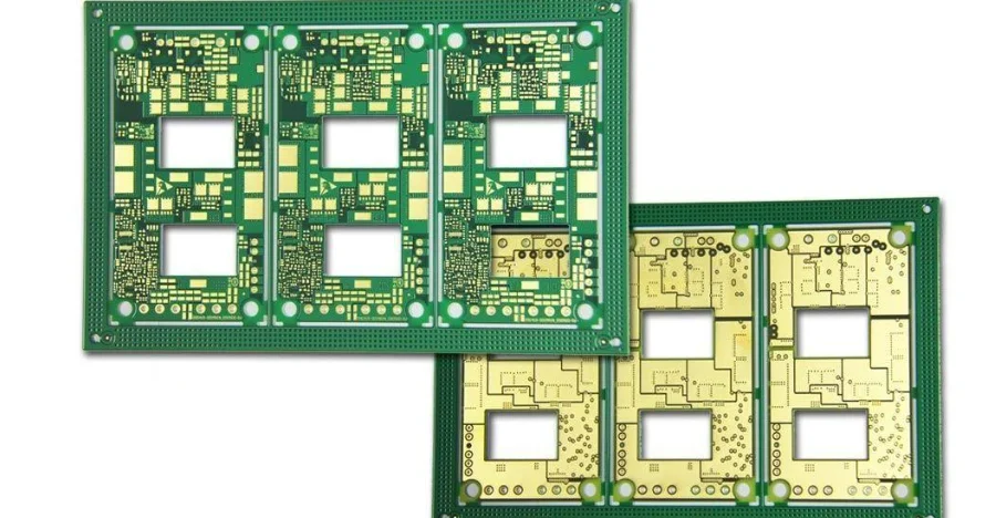
- JTAG and boundary-scan should be implemented as controlled engineering access methods for PCB test, debug, programming, and verification. They are not standalone cybersecurity controls.
- The first design reviews should confirm device support for IEEE 1149.1 boundary-scan, available physical test access, production debug rules, and manufacturing record requirements.
- IEEE 1149.1 defines a Test Access Port (TAP) and boundary-scan architecture that allows engineers to test digital interconnects, evaluate supported integrated circuits, and control specific device functions during operation.
- For medical electronics, debug access decisions should be connected to documented quality, manufacturing, and cybersecurity processes rather than treated as independent compliance evidence.
- Common first-build problems include incomplete scan-chain planning, inaccessible test points after packaging changes, missing programmed-state records, and inconsistent debug settings between prototype and production units.
JTAG and boundary-scan provide standardized access for testing PCB interconnects, inspecting supported device states, and performing controlled programming or debug operations through a Test Access Port. In medical imaging and wearable PCBs, their value comes from improving test coverage on dense assemblies when combined with proper manufacturing controls, traceability, and lifecycle planning.
Contents
- What to review first on a medical or wearable JTAG design
- Key design and validation rule table
- Early trade-off table
- How test access, dense packaging, and build records fit together
- How to control debug access without overclaiming compliance
- What prototype and pilot teams should freeze before release
- FAQ
- Next steps
- References
- Author and review
What to review first on a medical or wearable JTAG design
Medical imaging systems and wearable devices often place processors, FPGAs, sensors, memory devices, power-management ICs, and high-density connectors into very limited PCB space. As package density increases, direct electrical probing becomes more difficult, especially for BGA devices and components with hidden solder joints.
Boundary-scan helps solve access limitations, but only when the design team plans for it early. JTAG is not a replacement for all PCB testing, and it does not automatically provide security or regulatory compliance.
The first engineering review should confirm:
- whether processors, FPGAs, controllers, and other target devices support IEEE 1149.1 boundary-scan or vendor-specific JTAG functions
- whether the PCB layout includes suitable headers, test pads, or fixture access before mechanical packaging is finalized
- whether non-JTAG components have appropriate coverage through AOI, X-ray inspection, ICT, flying probe, or functional testing
- whether firmware loading, calibration programming, configuration settings, and debug states are captured in production records
- whether quality documentation clearly separates engineering access requirements from approved production behavior
For compact wearable layouts and medical imaging modules, HDI PCB, rigid-flex PCB, and turnkey assembly decisions should include test access requirements before the final stack-up, enclosure, and assembly process are locked.
A common mistake is designing the PCB first and adding test access later. Once shielding, batteries, connectors, and mechanical structures are finalized, adding JTAG access points may require expensive layout changes or fixture redesign.
Key design and validation rule table
| Rule / parameter | Recommended range or decision method | Why it matters | How to verify | If ignored |
|---|---|---|---|---|
| Device support check | Confirm actual device-level boundary-scan and debug capabilities before schematic release | JTAG functionality depends on silicon support, not only connector availability | Datasheet review and scan-chain definition review | The PCB may include access hardware that cannot perform the intended test |
| Test-access planning | Define headers, pads, or factory fixture access before mechanical freeze | Dense assemblies can eliminate physical access after packaging decisions | PCB layout review and fixture review | Production testing and failure analysis become difficult |
| Mixed-test strategy | Combine JTAG with AOI, X-ray, ICT, flying probe, or FCT where required | Boundary-scan only covers supported digital functions and interconnects | Manufacturing test coverage review | Teams may incorrectly assume JTAG provides complete PCB validation |
| Debug control policy | Define when JTAG is enabled, restricted, authenticated, or disabled | Engineering access requirements differ from deployed product requirements | Manufacturing procedure review and release approval | Prototype and production units may leave manufacturing in inconsistent states |
| Record traceability | Store programmed state and configuration data with unit serial records | Medical products require repeatable build history and failure-analysis capability | MES review or manufacturing log review | Field investigation cannot determine shipped hardware configuration |
| Claims discipline | Match security and compliance statements to documented controls | Technical claims must be supported by evidence | Quality review and regulatory documentation review | External claims may exceed actual product controls |
Early trade-off table
| Design choice | Usually stronger for | Main trade-off | What to confirm early |
|---|---|---|---|
| Full debug header access | Fast prototype development, firmware debugging, and failure analysis | Requires additional PCB area and stronger production controls | Mechanical clearance and manufacturing access policy |
| Limited pogo or factory-only access | Compact product designs and controlled production environments | Reduces convenience during engineering investigation | Fixture design and service requirements |
| Always-open production debug | Faster field service in some applications | Creates additional access-control and traceability concerns | Product risk assessment and service model |
| Controlled lock or disable after build | Better separation between manufacturing and deployed operation | Requires documented programming flow and recovery planning | Serial-level records and approved recovery procedures |
How test access, dense packaging, and build records fit together
The primary reason engineers use boundary-scan on medical imaging and wearable PCBs is access. Modern assemblies frequently use BGAs, fine-pitch packages, stacked components, and rigid-flex structures where traditional probe-based testing cannot reach every connection.
A successful JTAG implementation depends on three areas: physical access, realistic test coverage, and manufacturing traceability.
1. Does the PCB maintain access after mechanical integration?
A test strategy created during schematic design can fail after enclosure development. Connectors, shields, batteries, thermal structures, and folded flex sections can block previously planned test points.
Before releasing the design, confirm:
- JTAG signals are routed according to device requirements
- test pads remain reachable by production fixtures
- fixture clearance matches the final assembly condition
- service and failure-analysis access requirements are documented
For complex medical electronics, test access should be treated as a PCB architecture decision rather than a late manufacturing detail.
2. Is JTAG being used only for faults it can detect?
Boundary-scan is effective for many digital interconnect problems, including open connections, short conditions, and certain device-level verification tasks on supported components.
However, it does not replace every manufacturing inspection method.
Examples of issues that may require additional testing include:
- solder voids inside BGA packages
- analog measurement accuracy
- sensor calibration errors
- battery performance issues
- mechanical assembly problems
- system-level performance failures
That is why medical and wearable products typically combine JTAG with X-ray inspection, AOI, electrical testing, calibration procedures, and functional verification.
3. Are programmed states linked to production records?
JTAG is often involved in programming firmware, device configuration, FPGA images, calibration parameters, or security-related settings.
Each serial-numbered unit should have a traceable record showing:
- programmed firmware version
- configuration status
- calibration data where applicable
- debug-access state
- device lock or fuse status when used
For pre-production reviews, Gerber viewer and BOM viewer checks can help identify design-data mismatches before manufacturing begins.
How to control debug access without overclaiming compliance
JTAG discussions often combine manufacturing access, cybersecurity, secure boot, and regulatory requirements. These topics are related but should not be treated as identical.
A JTAG interface is an access mechanism. Its security impact depends on the device architecture, firmware controls, production configuration, and operational policies surrounding it.
A controlled debug process should define:
- which development stages allow unrestricted engineering access
- when factory-only access is required
- whether authentication or controlled fixtures are needed
- whether production units ship with JTAG enabled, restricted, or disabled
- who can approve changes to debug configuration after release
The production state should be documented through approved manufacturing procedures and build records. Relying on informal engineering knowledge creates uncertainty during audits, investigations, or field failures.
FDA cybersecurity guidance for medical devices focuses on cybersecurity risk management, design documentation, and premarket information. Therefore, a JTAG policy should support the broader device security process rather than serve as a standalone compliance statement.
For dense medical assemblies, medical PCB planning must connect electrical design, manufacturing access, and quality documentation. HDI PCB and rigid-flex PCB choices should account for both assembly constraints and test requirements.
What prototype and pilot teams should freeze before release
JTAG and boundary-scan provide the most value when the access strategy is defined before the PCB reaches production.
A practical release checklist should include:
Supported-device map frozen
Confirm which devices participate in the scan chain and which components require separate inspection methods.Access method approved
Freeze header, test-pad, pogo fixture, and manufacturing access assumptions before enclosure and assembly decisions are finalized.Production debug policy documented
Define the debug state of shipped products and identify who can authorize changes.Traceability requirements defined
Record firmware, configuration, calibration, and debug information at the unit level.Coverage gaps reviewed
Verify that AOI, X-ray, ICT, flying probe, or FCT covers areas outside JTAG capability.
During development cycles, pcb prototype, quick-turn PCB, and small-batch assembly services can help teams validate access assumptions before moving into larger production builds.
FAQ
What is the first thing to check before adding JTAG to a medical PCB?
First verify that the selected devices support the intended boundary-scan or debug functions and that the PCB design provides practical physical access after packaging decisions are complete.
Can JTAG replace all other production tests?
No. JTAG is valuable for supported digital devices and interconnect testing, but it cannot replace inspection and validation methods for analog performance, mechanical issues, solder defects, calibration, or complete system behavior.
Is leaving JTAG enabled on shipped products always acceptable?
No. The production debug state should follow a documented engineering and risk-management decision. Some products may require restricted or disabled access after manufacturing.
Why is traceability important for JTAG-based manufacturing flows?
Because programming, configuration, calibration, and lock settings affect the actual hardware state. Unit-level records allow teams to reproduce configurations during failure analysis and quality investigations.
Does using JTAG prove medical cybersecurity compliance?
No. JTAG can support a controlled development and manufacturing process, but cybersecurity claims require evidence from the complete product design, software controls, risk process, and documentation system.
Next steps
For medical imaging and wearable PCB projects, the most effective next step is a combined design review covering device support, physical access, manufacturing test coverage, debug policy, and traceability requirements before the first production build.
HILPCB can support this workflow through:
- HDI PCB planning for high-density medical assemblies
- Rigid-flex PCB solutions for compact wearable packaging
- Turnkey assembly support for controlled programming and manufacturing records
- PCB prototype and quick-turn PCB services for rapid design-test iterations
- Request a quote when your PCB design, test access strategy, and manufacturing requirements are ready
References
- IEEE 1149.1 Working Group: Standard Test Access Port and Boundary-Scan Architecture
- XJTAG tutorial: What is JTAG and how can I make use of it?
- FDA guidance: Cybersecurity in Medical Devices
- FDA: PMA Quality System
- IPC: Ensuring Excellence, IPC-A-610
Author and review
Author: HILPCB Engineering Content Team
Reviewed by: HILPCB Test Engineering and Medical Electronics Review Team
Last updated: 2026-04-21