
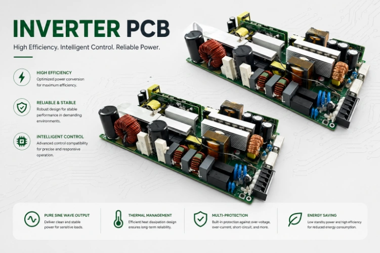
Every variable frequency drive spinning a factory motor, every solar inverter feeding the grid, every UPS system protecting a data center, and every induction cooktop heating a pan relies on a PCB converting DC to AC through high-frequency switching. The board carries gate drivers delivering 5–20 A peak current pulses in under 50 ns, routes DC bus connections carrying hundreds of amps through copper planes, and maintains ≥8 mm creepage between 600–1,500 V power circuits and control electronics operating at 3.3 V.
A gate drive layout error adding 2 nH of parasitic inductance causes IGBT shoot-through, both devices in a half-bridge conducting simultaneously, creating a short circuit across the DC bus that destroys the power module in microseconds. A thermal via array with 15% fewer vias than the thermal model specified causes the IGBT junction temperature to exceed 150°C at rated load, triggering thermal shutdown or derating the drive's output current by 20%. These aren't edge cases, they're the top two field failure root causes in industrial inverter products.
HILPCB manufactures inverter PCBs for VFD manufacturers, solar inverter companies, UPS system integrators, and industrial equipment OEMs worldwide. Our capabilities include heavy copper fabrication up to 10 oz, high-voltage isolation design, and multilayer constructions up to 64 layers. IATF 16949 process controls support automotive traction inverter programs.
Menu Navigation
- Gate Driver Layout: Where Efficiency Is Won or Lost
- DC Bus Architecture and Decoupling
- Current Sensing for Closed-Loop Motor Control
- High-Voltage Isolation and Safety Spacing
- Thermal Engineering at the Board Level
- Application-Specific Inverter Designs
Gate Driver Layout: Where Efficiency Is Won or Lost
The gate driver determines switching speed, switching loss, and susceptibility to parasitic turn-on (cross-conduction). For SiC MOSFETs at dV/dt >50 V/ns, gate loop inductance must stay below 5 nH. For IGBTs at 5–10 V/ns, the tolerance is larger but the consequences of gate oscillation are equally destructive. Device selection itself is covered in our IGBT vs MOSFET comparison.
Gate Drive PCB Rules
- Driver-to-Switch Proximity: Gate driver IC within 5 mm of the power device gate pin. Gate resistor (Rg_on = 1–5 Ω for SiC, 5–15 Ω for IGBTs; Rg_off = 2–10 Ω for SiC, 5–20 Ω for IGBTs) between driver output and gate pad. No layer transitions (vias) in the gate drive trace, each via adds 0.2–0.5 nH. Route gate and gate return on the same layer, side by side, forming a tightly coupled pair that minimizes loop area.
- Kelvin Source/Emitter Connection: Dedicated low-current return path from the MOSFET source or IGBT emitter, separate from the power path. The power source/emitter trace carries load current (potentially hundreds of amps) that creates di/dt-induced voltage drops. If this voltage couples into the gate drive return, it either fights the turn-on command (slowing switching and increasing loss) or assists parasitic turn-on during the complementary device's switching event.
- Isolated Gate Supplies: High-side gate drivers need isolated power supplies, typically bootstrap (for cost-sensitive designs) or isolated DC-DC (for reliability-critical designs). Bootstrap diode and capacitor placed within 3 mm of the driver IC. The bootstrap charging loop must be short to avoid ringing during the refresh cycle that occurs when the low-side device turns on.
- Dead-Time and Desaturation Routing: Dead-time signals between upper and lower gate drivers must be matched in propagation delay to prevent simultaneous conduction. Desaturation detection traces (monitoring the power device's collector-emitter or drain-source voltage during on-state) carry high-voltage signals that must be clamped and filtered before reaching the driver IC, routing these traces away from sensitive gate drive paths and analog current sense circuits.
- Common-Mode Transient Immunity: When the switching node transitions at 50 V/ns, the dV/dt across the isolation barrier of the high-side gate driver creates displacement current through the driver's isolation capacitance (typically 2–10 pF). This common-mode current flows through the gate driver's ground-to-switching-node parasitic capacitance. The PCB must provide a low-impedance return path for this current, connecting the driver's output ground directly to the MOSFET source with minimal trace length. A missing or high-impedance return path causes gate voltage glitches that trigger parasitic turn-on.
DC Bus Architecture and Decoupling
The DC bus provides energy for each switching cycle. At 600–1,500 V bus voltage and switching frequencies of 10–100 kHz, the bus capacitor bank supplies hundreds of amps of ripple current. Bus inductance and capacitor ESL determine the voltage overshoot at turn-off, directly affecting device stress, EMI emissions, and snubber requirements.
Bus Layout Engineering
- Planar Bus Construction on PCB: For inverters below 50 kW, heavy copper PCB planes (4–6 oz on external layers, 2–3 oz internal) can serve as the DC bus. Positive and negative bus planes on adjacent layers with thin dielectric (4–8 mil) between them form a distributed planar capacitor with sub-nH inductance per square centimeter. This geometry is inherently lower inductance than discrete bus bars for moderate current levels.
- Ceramic Decoupling at the Switching Node: Film bulk capacitors provide energy storage but have 10–20 nH mounting inductance. Ceramic capacitors (4.7–22 µF, X7R with DC bias derating carefully accounted for, a 22 µF X7R at 500 V DC bias may provide only 3–5 µF actual capacitance) placed directly at the half-bridge with <5 mm trace length provide the sub-10 nH decoupling needed for clean switching transitions.
- Three-Phase Symmetry: In three-phase inverters, each phase's decoupling layout must be electrically identical. Unequal bus inductance between phases causes different turn-off overshoot on each phase, leading to unbalanced power loss, differential EMI, and potentially exceeding the voltage rating on the phase with highest inductance.
- Bus Voltage Measurement: Resistive divider for bus voltage monitoring placed at the capacitor bank, not at the switching node where dV/dt transients corrupt the reading. The divider's midpoint trace routed as a shielded analog path to the MCU's ADC, filtered through an RC low-pass (100 kHz cutoff typical) to reject switching noise.
Current Sensing for Closed-Loop Motor Control
Phase current measurement enables field-oriented control (FOC) for motor drives and grid synchronization for grid-tie inverters. Measurement accuracy directly affects torque ripple, efficiency, and THD, a 1% current offset produces a 1% torque ripple that may be audible in quiet motor applications.
Sensing Techniques and Layout
- Inline Shunt Resistors: 0.1–2 mΩ metal element shunts on the low-side return path. Kelvin sense traces routed differentially on an internal layer, shielded from switching node dV/dt by a ground plane. PCB copper resistance in the sense path adds temperature-dependent measurement error, the copper trace resistance changes at 0.39%/°C, so a 0.5 mΩ trace resistance at 25°C becomes 0.7 mΩ at 75°C, adding 40% measurement error if not calibrated out.
- PCB-Integrated Rogowski Coils: Spiral copper traces on an internal multilayer PCB layer surrounding the phase conductor, providing contactless, isolated current measurement with inherent galvanic isolation. HILPCB fabricates these coils with ±0.05 mm trace positioning accuracy for consistent sensitivity (V/A) across production lots. Rogowski coils measure di/dt (rate of change of current), requiring an integrator circuit on the PCB to recover the current waveform.
- Hall-Effect Current Sensors: Discrete sensors (Allegro ACS772, LEM LTSR) mounted in the PCB with the power conductor passing through or near the sensor element. The sensor's output (analog voltage proportional to current) routes to the MCU's ADC through an anti-aliasing RC filter. Physical placement and conductor geometry affect measurement linearity and offset, controlled by PCB slot width and sensor positioning accuracy.
- ADC Interface: Current sense signals routed as differential pairs to the MCU's ADC inputs. Anti-aliasing filter (RC low-pass, typically 10–50 kHz cutoff) placed within 3 mm of the ADC input pins, not at the shunt, where long filtered traces would pick up switching noise. Phase-to-phase matching of filter components within ±0.1% for balanced three-phase measurement.
High-Voltage Isolation and Safety Spacing
Inverters operate at 400–1,500 V DC bus. Safety standards, IEC 62477-1 (power converter systems), UL 61800-5-1 (adjustable speed drives), IEC 62109-1 (solar inverters), define isolation and spacing requirements.
Isolation on the PCB
- Creepage and Clearance: At 800 V working voltage, reinforced insulation on Material Group IIIb laminate requires ≥10 mm creepage per IEC 60664-1. High-CTI laminates (CTI ≥ 600) reduce this requirement, enabling compact designs that wouldn't be physically possible on standard FR-4. HILPCB stocks automotive-grade high-CTI laminates from Isola and Panasonic.
- Slot Isolation: CNC-routed slots (2.0–3.0 mm) between high-voltage power and low-voltage control sections. Slot edge quality controlled to prevent exposed glass fibers that create surface tracking paths under humidity. Solder mask pullback from slot edges provides additional protection.
- Isolation Component Interface: Optocouplers, capacitive isolators, and gate drive transformers straddling the safety boundary, their PCB footprints aligned with the slot or creepage gap. Package standoff height and pin-to-pin spacing verified against the isolation voltage rating.
- Production Hi-Pot Test: 100% of production boards tested at rated test voltage (typically 2 × working voltage + 1,000 V AC) for 60 seconds. This catches manufacturing defects, solder balls, flux bridges, under-etched copper, that reduce effective creepage below the designed value.
Thermal Engineering at the Board Level
Power devices in inverters dissipate 50–500 W total. The PCB is part of the thermal path between semiconductor junction and heatsink, its thermal resistance directly affects the inverter's continuous power rating.
Thermal Design
- Thermal Via Arrays: 0.3 mm drill, 0.6 mm pitch, copper-filled vias under power device thermal pads. Filled vias: <5 °C/W. Open vias: 10–15 °C/W. The difference directly affects how much current the inverter can deliver continuously.
- Heavy Copper Planes: Internal heavy copper (2–4 oz) serves as lateral heat spreader. A 2 oz copper plane spreads heat from a 10 × 10 mm hotspot across a 50 × 50 mm area, reducing peak temperature by 15–25°C compared to 1 oz copper.
- High-Tg Materials: Tg ≥ 170°C for continuous high-temperature operation. Standard FR-4 approaching its Tg becomes mechanically soft and dimensionally unstable, leading to solder joint fatigue and delamination over the inverter's 15–20 year service life.
- Copper Coin Inserts: For highest thermal performance, HILPCB presses machined copper slugs into board cavities directly under power devices, achieving <1 °C/W thermal resistance through the board thickness. Available on boards up to 64 layers.
Application-Specific Inverter Designs
- Solar Micro-Inverters: Single-phase, 250–500 W, potted in epoxy for outdoor installation on solar panel frames. 25-year warranty life requiring extreme reliability. Components and PCB materials selected for 100,000+ thermal cycles (-40°C to +85°C). Board surface finish compatible with potting compound adhesion. Rooftop PV systems also need DC arc fault detection, which is often built into the inverter board.
- Industrial VFDs: Three-phase, 400 V or 690 V bus, 1–500 kW. Modular power stage boards designed for parallel operation. Standard mounting holes, bus bar interfaces, and control connectors enabling scalable platforms where the same PCB design serves multiple power ratings by changing the number of paralleled modules.
- UPS Systems: Online double-conversion topology with two complete power stages, rectifier (AC→DC) and inverter (DC→AC), sharing a DC bus. Battery charger function integrated on the rectifier board. Transfer switch control with <10 ms switchover time requiring deterministic control signal routing.
- Induction Heating/Welding: Resonant inverters at 20–200 kHz, current levels reaching 500–1,000 A in the resonant tank. Litz wire connections to the PCB through high-current terminal blocks. Resonant capacitor mounting with vibration-dampened mechanical design, film capacitors under high-current AC excitation generate acoustic noise and mechanical vibration.
Submit your inverter PCB design for thermal simulation and DFM review →
Frequently Asked Questions
Why must the gate driver be placed so close to the SiC MOSFET or IGBT? Power devices like SiC MOSFETs switch at extremely high speeds (>50 V/ns). Any parasitic inductance in the trace between the gate driver and the switch (even 5 nH) can cause severe gate ringing. This ringing can lead to parasitic turn-on (shoot-through), which causes a short circuit across the DC bus and destroys the module.
What is a Kelvin source connection on an inverter PCB? A Kelvin source provides a dedicated, low-current return path directly from the MOSFET source to the gate driver. It isolates the gate drive circuit from the main power path, ensuring that massive voltage drops caused by high-current switching (di/dt) don't interfere with or accidentally trigger the gate.
How do you achieve 800V isolation on an inverter circuit board? To safely separate 800V power circuits from 3.3V control electronics, the PCB must maintain strict creepage distances (often ≥10 mm on standard FR-4). HILPCB achieves this using CNC-routed isolation slots to physically separate the sections, and by using high-CTI (Comparative Tracking Index) laminates that resist electrical tracking across the surface.
How does an inverter PCB handle hundreds of amps of current? For inverters under 50 kW, heavy copper fabrication (4–6 oz on outer layers, 2–3 oz internally) can be used to construct planar busbars directly within the PCB. To handle the massive heat generated by this current, the board utilizes copper-filled thermal via arrays and embedded copper coins to conduct heat directly from the power devices into an external heatsink.
What should an inverter power-module layout verify?
An inverter board can contain power switching, gate drive, sensing and control functions. For a selected power module, use its pinout and recommended commutation loop, DC-link connection and insulation requirements; keep the loop low-inductance and verify cooling and protection. Heavy copper or busbars are options where the current path justifies them, not requirements for every controller board.