
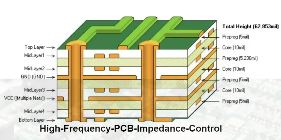
In modern hardware design, PCB traces are no longer just simple connecting wires; they are complex high-frequency transmission lines. As interface speeds skyrocket from 1Gbps (like Gigabit Ethernet) to 112Gbps (PAM4 modulation), the selection of PCB materials and the design of the stack-up (Stack-up) have become the decisive factors in whether a product succeeds or fails. A poorly designed stack-up can lead to severe signal integrity (SI) issues, catastrophic Electromagnetic Interference (EMI), and even manufacturing failures.
This low loss laminate tutorial is designed for hardware engineers, PCB layout designers, and engineering managers. We will comprehensively decode the core parameters of materials, explore PCB stackup guide strategies for different application scenarios, and reveal the delicate balance between impedance, thermal reliability stackup, and cost. Our goal is to help your team establish a standardized, reliable stack-up library, transforming the "black magic" of PCB design into predictable engineering.
1. Demystifying materials: The physics of Dk, Df, and Tg
Before diving into stack-up design, we must understand the fundamental physical properties of PCB materials. Why can't standard FR-4 handle high-speed signals? The answer lies in the interaction between the dielectric material and electromagnetic waves.
The dual characteristics of Dielectric Constant (Dk)
The Dielectric Constant (Dk), also known as Relative Permittivity, describes a material's ability to store electrical energy within an electric field. In high-speed PCB design, Dk acts as a double-edged sword:
- Impact on Impedance: A higher Dk results in a higher capacitance between the trace and the reference plane, leading to a lower characteristic impedance (Z0). To maintain a 50Ω impedance, a higher Dk requires a thicker dielectric layer or a narrower trace width.
- Impact on Propagation Speed: Electromagnetic waves travel slower in materials with higher Dk. The propagation delay (tpd) is proportional to √Dk. When designing precisely length-matched differential pairs or memory buses (like DDR), variations in Dk directly cause timing skew.
- Frequency Dependency: Dk is not a constant. It decreases as signal frequency increases. High-end materials exhibit a flatter Dk vs. frequency curve, ensuring consistent impedance and timing across a wide bandwidth.
Dissipation Factor (Df): The invisible killer of signal energy
The Dissipation Factor (Df), also known as Loss Tangent (tan δ), measures how much electromagnetic energy is converted into heat (dielectric loss) as a signal passes through the material.
- Dielectric Loss \propto Frequency × Dk × Df. This formula reveals a cruel reality: as frequency doubles, dielectric loss doubles; if you choose a material with a high Df, the loss increases linearly.
- For high-speed serial links (like PCIe 5.0 at 32GT/s), severe dielectric loss will collapse the signal eye diagram, causing the receiver to be unable to recover the data. Therefore, the core of this
low loss laminate tutorialis selecting materials with a sufficiently low Df.
Glass Transition Temperature (Tg) & Reliability
While Dk/Df determine electrical performance, thermal and mechanical parameters dictate if the board can be successfully manufactured and operate long-term.
- Tg (Glass Transition Temperature): The temperature at which the resin transitions from a rigid, glassy state to a soft, rubbery state. A high Tg (typically >170°C) means the material maintains its mechanical strength and dimensional stability at higher temperatures (like during lead-free reflow soldering), reducing the risk of via barrel cracking.
- CTE (Coefficient of Thermal Expansion): Especially in the Z-axis (thickness direction). Since copper's CTE is much lower than resin's, excessive Z-axis expansion during heating generates immense stress on plated through-holes (PTH), leading to failures. Building a robust
thermal reliability stackuprequires selecting materials with low Z-axis CTE.
2. Material grades: From Standard FR-4 to Ultra-Low Loss
The industry typically classifies PCB materials based on their Df values at 10GHz. Understanding these grades is crucial for cost-effective material selection.
| Grade | Typical Df Range | Representative Materials | Typical Applications |
|---|---|---|---|
| Standard FR-4 | 0.015 - 0.025 | Shengyi S1000-2, IT-180A | Consumer electronics, low-speed digital (<3Gbps), power boards |
| Mid Loss | 0.008 - 0.012 | TU-862HF, S1000-2M | PCIe Gen 3, 10G Ethernet, DDR4 |
| Low Loss | 0.005 - 0.008 | Panasonic Megtron 4, TU-872SLK | PCIe Gen 4, 25G NRZ, core routers |
| Very Low Loss | 0.003 - 0.005 | Megtron 6, IT-968, Tachyon 100G | PCIe Gen 5, 56G PAM4, 400G switches |
| Ultra Low Loss | < 0.003 | Megtron 7, Rogers 4000 series, PTFE | PCIe Gen 6, 112G PAM4, 77GHz automotive radar |
Note: Dk and Df values vary with resin content and glass weave styles. Always consult the manufacturer's specific datasheet during design.
Selection Strategy: Don't blindly pursue top-tier materials. High-end materials are not only expensive but often require specialized manufacturing processes (like plasma desmearing). A good engineer chooses the material that just meets the loss budget, balancing performance, cost, and manufacturability.
3. PCB Stackup Guide: Classic structures from 4 to 12 layers
Stack-up design is an art of managing space. The goal is to allocate Signal (S), Power (P), and Ground (G) layers reasonably within a limited thickness to optimize impedance, cross-talk, and EMI. Here are several classic PCB stackup guide templates.
4-Layer Board: The fundamental compromise
- Classic Structure: Top (S) - Inner 1 (G) - Inner 2 (P) - Bottom (S)
- Advantages: Simple, low cost. Inner ground and power planes provide good low-frequency decoupling and EMI shielding for surface signals.
- Disadvantages: The distance between power and ground is usually large (typically 40 mils in a standard 62 mil board), resulting in low inter-plane capacitance, poor high-frequency decoupling. Not suitable for dense high-speed routing.
6-Layer Board: The starting point for high-speed design
A 6-layer board offers more flexibility. The focus is ensuring critical high-speed signals have an uninterrupted ground reference.
- Structure A (Preferred): Top (S) - G - Inner 1 (S) - Inner 2 (S) - P - Bottom (S)
- Pros: Inner 1 and 2 are shielded.
- Cons: Inner 1 references Ground, Inner 2 references Power. If signals transition between these layers, the return path is broken, requiring stitching capacitors.
- Structure B (High SI/EMI focus): Top (S) - G - Inner 1 (S) - P - G - Bottom (S)
- Pros: Power and Ground are adjacent, providing excellent high-frequency decoupling. All signal layers have adjacent reference planes.
8-Layer Board: Standard for servers and high-end industrial
For complex systems with multiple voltage rails (like FPGAs or SoCs) and extensive high-speed interfaces (like DDR, PCIe).
- Classic Symmetrical Structure: Top (S) - G - Inner 1 (S) - P - G - Inner 2 (S) - G - Bottom (S)
- Analysis: This is an extremely robust structure. Inner 1 and Inner 2 are configured as striplines (sandwiched between two solid planes), providing the best impedance control and lowest cross-talk. The adjacent P and G planes offer excellent power integrity.
10/12-Layer and Above: High-density and multi-plane
As layer counts increase, the core principle remains: Ensure critical signal layers (especially striplines) have adjacent, uninterrupted ground planes. For complex power designs, multiple P-G pairs can further improve signal isolation and power integrity. For HDI designs, these layers can accommodate numerous microvias, blind vias, and buried vias.
4. Synergy of Signal/Power/Ground/Copper Thickness
The soul of an excellent stack-up lies in the synergy between its layers.
-
Prioritize Reference Plane Integrity
High-speed signal layers must be immediately adjacent to a solid ground or power plane. Avoid routing signals across splits in the reference plane, as this is the primary culprit for cross-talk and EMI.
-
Route High-Speed Signals on Inner Layers
Inner stripline structures (GND-SIG-GND) offer superior EMI shielding and impedance control stability compared to surface microstrip lines (SIG-GND).
-
Tightly Couple Power and Ground Planes
Place main power and ground planes adjacent to each other to utilize the planar capacitance formed between them. This provides a low-impedance return path for high-frequency currents, significantly enhancing power integrity.
-
Trade-offs in Copper Thickness
Standard signal layers typically use 0.5oz (18μm) or 1oz (35μm) copper. 0.5oz allows for finer trace widths and spacing, ideal for high-density designs. High-current power layers may require 2oz (70μm) or thicker copper, demanding a reliable thermal reliability stackup design.
-
Symmetrical Structure to Prevent Warpage
The stack-up design should be as symmetrical as possible, top-to-bottom, regarding materials, copper thickness, and copper distribution. Asymmetrical designs tend to warp during lamination and reflow soldering due to unbalanced thermal stresses.
5. Hybrid lamination & Special materials: When standard isn't enough
Sometimes, a single material cannot meet all requirements, for example, a board containing both RF signals and digital control circuitry. In such cases, hybrid lamination must be considered.
| Strategy | Advantages | Disadvantages | HILPCB Recommendation |
|---|---|---|---|
| Pure Low Loss Material | Consistent performance, mature manufacturing process | High cost | Suitable for telecom and server products demanding extreme performance. |
| Rogers + FR-4 Hybrid | Balances RF performance with digital circuit cost | Complex lamination parameters, reliability risks, CTE mismatch | Suitable for integrated antenna designs. HILPCB has extensive hybrid experience to optimize lamination profiles and ensure reliability. |
| MCPCB (Metal Core) | Exceptional thermal dissipation | Limited to single/double-layer, cannot support complex routing | Suitable for high-power LED lighting and power modules where thermal management is critical. |
| Rigid-Flex | Enables 3D interconnects, high reliability | Complex design, very high cost | Suitable for wearables and aerospace applications with strict space and reliability constraints. |
6. Manufacturing impact: The "last mile" from design to physical PCB
A theoretically perfect stack-up can lead to soaring costs or plummeting yields if Design for Manufacturability (DFM) is ignored.
- Resin Flow & Press Cycle: We precisely control the temperature and pressure profiles during lamination based on the specific type of Prepreg (PP) you select. For instance, high-resin-content 106 PP requires precise control to fill HDI laser microvias without excessive resin loss, which could lead to uncontrolled dielectric thickness.
- Fiber Weave Effect: For signals above 25Gbps, the loose weave of standard glass cloth (like 7628) causes local Dk variations, affecting impedance. HILPCB recommends and stocks flat-glass low loss laminates to significantly improve signal quality.
- Back-drilling: Via stubs are "killers" of high-speed signals. For >10Gbps signals, we offer precision depth-controlled back-drilling to remove unused stubs, reducing insertion loss by 1-2dB.
- Impedance Coupons & TDR Testing: Every production batch includes impedance test coupons. HILPCB's lab utilizes Time Domain Reflectometry (TDR) for precise measurements, ensuring your final product's impedance falls within your specified tolerances (±10% or tighter).
- Surface Finish Comparison: Surface finishes also impact high-speed signals. Electroless Nickel Immersion Gold (ENIG) is flat and suitable for high frequencies, but carries a "black pad" risk and higher cost. Organic Solderability Preservative (OSP) is cost-effective but has a shorter solderability shelf life. We provide optimal surface finish recommendations based on your application and cost targets.
7. How HILPCB can help you master stack-up design
After reading this low loss laminate tutorial, you might still find stack-up design challenging. That's exactly why the HILPCB Stack-up & Material Academy exists. We are not just a manufacturer; we are your engineering partner.
We've launched a "Fast Stack-up Claim" service designed to free you from tedious material selection and stack-up calculations.
Not sure where to start? Let HILPCB engineers customize your stack-up
Simply provide your design requirements (data rate, layer count, impedance targets, etc.), and our senior engineers will deliver a professional, DFM-verified, and material-inventory-optimized stack-up proposal within 24 hours, complete with a detailed impedance calculation report. Completely free!
Why choose HILPCB?
- 200+ Materials in Stock: We stock a full range of materials from standard FR-4 to high-end Rogers and Megtron series, preventing project delays caused by special material MOQs and long lead times.
- Experienced Engineering Team: Our engineers have handled thousands of high-speed, high-frequency, and high-density projects. They can quickly identify potential risks and provide optimized solutions that balance performance and cost.
- Advanced Impedance Testing Lab: We don't just promise impedance control; we verify it through rigorous TDR testing, ensuring every board you receive meets your design specifications.
Summary
Successful stack-up design is a delicate balancing act between performance, cost, and manufacturability. We hope this tutorial provides a clear framework. Remember: start by defining your input conditions, use material parameter tables for initial selection, apply proven stack-up paradigms, and always maintain open communication with your PCB manufacturer (like HILPCB) to bring manufacturing constraints forward into the design phase. This approach will help your team build a standardized, reliable stack-up library and accelerate the product development process.
Common Questions
What inputs should a team lock before choosing a low-loss laminate?
Teams should first lock the data rate, channel length, insertion-loss budget, target impedance, layer count, thermal requirements, and cost target. Those boundary conditions determine whether standard FR-4 is enough or whether a Mid-Loss, Low-Loss, or Ultra-Low-Loss material is justified.
When is standard FR-4 no longer enough for a high-speed PCB?
Standard FR-4 usually stops being comfortable once links become longer, the loss budget gets tight, or the design moves into higher-speed classes such as 56G, 112G, PCIe 5.0, or PCIe 6.0. At that point, engineers typically need lower Df materials, tighter impedance control, and stronger manufacturing discipline.
How should engineers balance low-loss performance, stack-up, and manufacturability?
The best approach is to choose materials together with the stack-up and the fabricator's real process window. Copper weight, dielectric thickness, lamination behavior, back-drill needs, and coupon verification all have to work together, otherwise a theoretically strong material choice can still create cost or yield problems.
Conclusion
In conclusion, this article serves as a comprehensive low loss laminate tutorial, detailing material parameters, stack-up planning, impedance/thermal/cost trade-offs, and manufacturing considerations. Complete with comparison tables and examples, it is designed to help teams systematically manage risks in design, material selection, and testing, facilitating the creation of standard stack-up libraries. By following the checklists and process windows outlined here, and by engaging HILPCB's DFM/DFA team early on, you can significantly accelerate prototype and mass production delivery while guaranteeing quality and compliance.
For manufacturing and assembly support, contact HILPCB for Turnkey Assembly or SMT Assembly to get DFM/DFT advice.