

Ceramic PCB Assembly Process and Best Practices
Ceramic PCB assembly depends on metallization, package geometry, measured reflow profiles and joint acceptance. Match the SMT or hybrid route to thermal, RF and sourcing requirements.
Expert insights on PCB manufacturing, assembly excellence, and cutting-edge electronic technologies
Your trusted partner for professional PCB manufacturing and assembly solutions
Ceramic PCB assembly depends on metallization, package geometry, measured reflow profiles and joint acceptance. Match the SMT or hybrid route to thermal, RF and sourcing requirements.
Design environmental monitoring PCBs around sensor noise, condensation, heater power and calibration. Compare practical board options and prepare a manufacturing RFQ.

Plan LED PCB assembly with package-specific paste, void inspection, measured reflow and optical alignment. Define MCPCB, COB and functional-test handoff requirements.
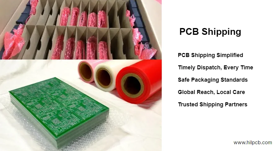
Learn how to ship PCBs safely and affordably. Discover the best carriers, packaging methods, customs documentation, and cost-saving strategies for domestic and international PCB logistics.
Explore edge AI and IoT gateway PCB design for predictive analytics, covering sensor interfaces, wireless protocols, signal integrity, thermal budgets and manufacturability.
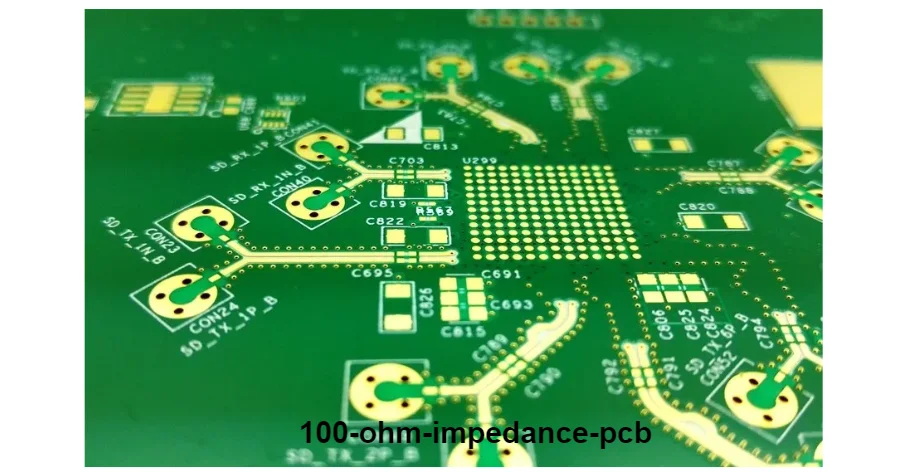
1000BASE-T1 PCB design controls the nominal 100-ohm differential MDI path, balance, return loss and EMC while matching materials and manufacturing evidence to the vehicle program.

Turnkey HDMI PCB assembly from prototype to volume. SMT and through-hole HDMI connectors, AOI/X-ray inspection, and testing support.
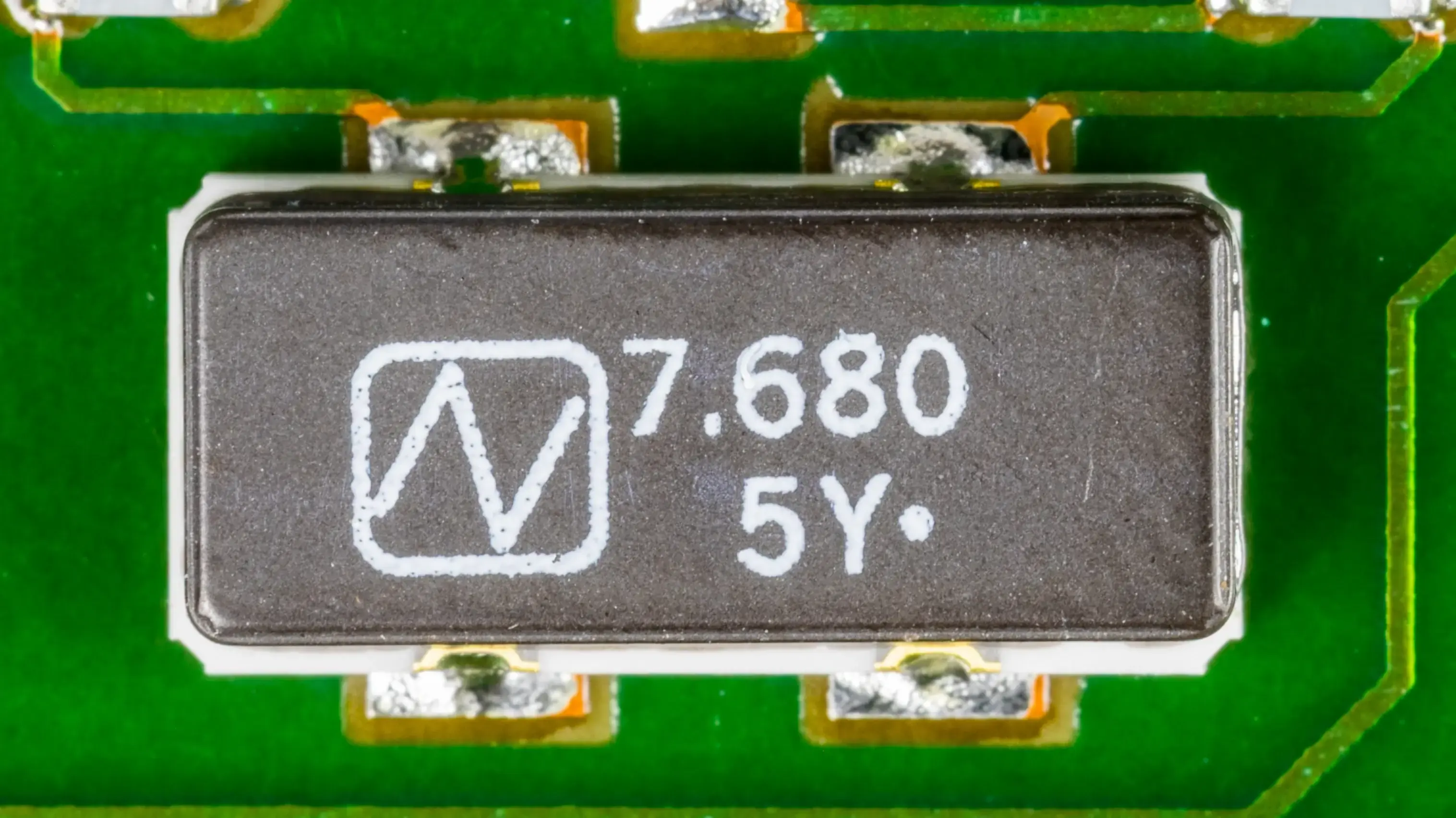
Practical THz communication PCB guide for 6G research hardware, covering sub-THz frequency boundaries, low-loss materials, GCPW/SIW routing, AiP transitions, PDN, thermal design, precision manufacturing, test coupons and RFQ handoff.
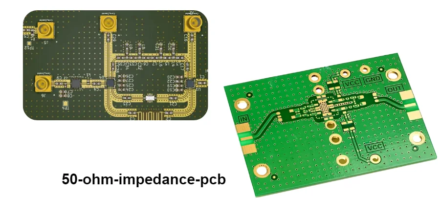
50-ohm RF PCB manufacturing coordinates stackup, trace geometry, material properties and impedance coupons with the channel budget and agreed fabrication tolerances.
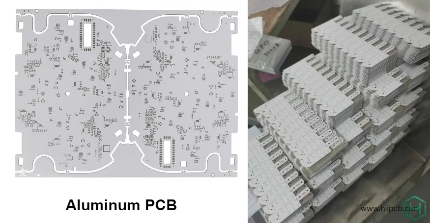
Comprehensive guide on aluminum PCB technology — covering working principles, thermal advantages, materials, design guidelines, applications, and manufacturing capabilities for high-power electronics.
EMC analyzer PCB design coordinates receiver linearity, noise, clocking, RF channels and calibration interfaces; measured uncertainty and test configuration determine usable results.
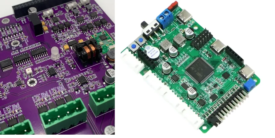
Design welding robot PCBs with clear controller and power-source boundaries, EMC control, functional-safety evidence, harsh-environment tests and RFQ guidance.