
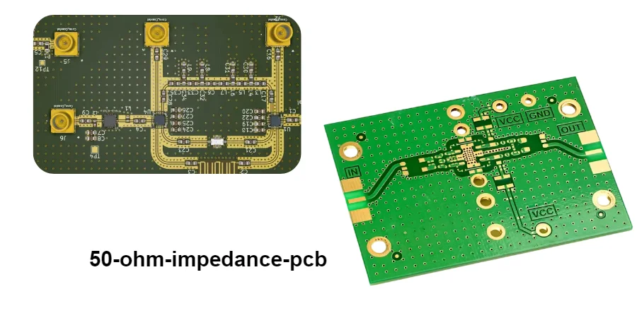
A 50-ohm RF PCB uses controlled transmission-line geometry to connect circuits designed for a nominal 50 Ω reference. Matching that reference helps limit reflections, but acceptable performance also depends on connectors, transitions, loss and the operating frequency band.
A successful 50 Ω RF board depends on its stackup, conductor geometry, reference planes, transitions and verified materials. Confirm fabrication tolerances, available measurement methods and manufacturing sites against a project-specific quotation rather than an unqualified capability guarantee.
Quality 50-Ohm PCB Manufacturing with Cost Control
Balancing premium RF performance with cost efficiency in 50-ohm impedance PCB manufacturing requires a systematic approach that integrates engineering precision, material optimization, and lean production management. The effect of an impedance deviation depends on its magnitude, electrical length and the channel return-loss budget; a 2–3 Ω deviation is not a universal pass/fail limit.
1. Engineering for Manufacturability (DFM/DFA)
A DFM review should reconcile trace width calculations for target impedance with the fabricator’s finished copper and dielectric construction. Review reference planes, via transitions, connector launches and SMT assembly access together. Use a field solver or electromagnetic model where launches and discontinuities exceed the accuracy of a uniform-line calculator; agree who supplies the model and how it will be checked on the prototype.
2. Strategic Material Selection and Sourcing
Substrate cost can be a major part of a 50-ohm PCB quotation. For a high-frequency PCB, specify the laminate grade, dielectric thickness, copper foil, substitution rule, and required documents. If RO4003C, RT/duroid, or another Rogers material is required, HILPCB confirms availability, procurement lead time, and source evidence for that build before order release.
3. Process Optimization and Automation
Trace width, finished plating thickness and dielectric height have correlated effects on impedance. Agree achievable tolerances with the fabricator using the intended panel and stackup; a universal ±0.5 mil line-width or ±5% dielectric-height guarantee is not supportable without process data.
4. Panel Utilization and Yield Management
Panelization must leave space for representative impedance coupons, assembly rails and tooling while respecting RF-edge and connector requirements. Multi-product panels may share setup costs when material, stackup and processing are compatible; their coupon and lot traceability must still identify the represented boards. Review measured variation across the intended panel before using yield assumptions in a volume quotation.
5. Quality Assurance with Performance Focus
RF verification may combine representative TDR impedance coupons, calibrated S-parameter measurements and loss characterization when required by the customer. Define coupon structures, sampling and acceptance bands in the build specification; not every production board receives complete RF network analysis.
Compare quotations using the same stackup, tolerance, sampling and report requirements so a lower price does not silently remove an acceptance check.
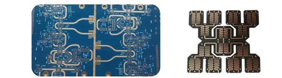
Managing Signal Integrity in High-Frequency 50-Ohm PCB Design
50 Ω is a common single-ended RF-system reference, not a universal target for every digital or differential trace. Interconnect design must follow each interface specification, transition geometry, frequency band and loss/return-loss budget.
Key signal-integrity checks for a 50-ohm PCB include:
- Pre-layout electromagnetic simulation to optimize trace geometries and layer stackups
- Controlled dielectric selection with stable Dk and low loss tangent for frequency stability
- Precision copper plating to maintain consistent trace cross-sections
- Via transition optimization including anti-pad design and back-drilling where the modeled stub affects the channel budget
- Reference plane management ensuring continuous ground planes for stable impedance
- Manufacturing feedback: Confirm impedance tolerances for the actual stackup, sample size and frequency range; values such as ±3% must be substantiated by process capability and measured coupons.
These checks address discontinuities and return paths; final insertion loss, return loss and emissions still depend on the populated circuit and enclosure. Texas Instruments’ High-Speed Interface Layout Guidelines, Rev. J, sections 2.4 and 3.6, illustrate reference-plane and via-stub mechanisms; its device-specific dimensions are not universal RF-board limits.
Accelerating Time-to-Market for RF Product Development
HILPCB offers 50-ohm engineering, fabrication and assembly support, including DFM and trace/reference design, electromagnetic simulation, ±0.5 mil trace-width tolerance and dielectric-thickness variation of less than 5% in either direction, and tighter ±3% impedance routes where the released construction qualifies. Process options include AOI, SPC, plating/etch/lamination control, CAD panel and coupon optimization, multi-project panels and 3–5-day prototypes. TDR and RF S-parameter testing up to 40 GHz, thermal-cycle/shock, humidity and mechanical tests, RF records, custom stackups and PTFE/thermal integration can be scoped. Turnkey prototype-to-volume support covers antennas, RF modules, shielding, test fixtures, power, digital/interconnect and regulatory documentation; agree methods and combinations in the quote. In HILPCB’s recorded early engineering collaboration experience, re-spin rates were reduced by over 35%; this historical, context-specific result is not a guaranteed reduction for a new project.
Speed as Competitive Advantage
In RF and microwave markets—especially 5G infrastructure and automotive radar—development cycles are compressed, and early market entry can determine product success. Design iteration delays can mean missing critical design-in opportunities or losing competitive positioning.
Integrated Development Workflow
A practical development schedule separates these deliverables:
- Early Impedance Modeling — agree the stackup and model assumptions before prototyping
- Prototype Build — quote timing after material availability, tooling, assembly and required inspection are known
- RF Performance Validation — specify coupon TDR, populated-board S-parameters or other tests, including calibration planes, fixtures, frequency range and acceptance limits
Reduced Development Risk
Coordinate fabrication, assembly and RF testing around one revision-controlled build package. Identify which supplier performs each test and supplies the fixture and reports; fabrication and assembly in a single order do not imply complete RF-system validation.
Market Responsiveness
Use each prototype review to:
- Synchronize product launches with market windows
- Respond quickly to customer specification changes
- Iterate designs rapidly based on system-level testing
- Reduce overall development costs through faster convergence
Customization for Specialized RF Applications
50-ohm impedance requirements extend across diverse RF applications—from consumer wireless devices to military radar systems. Each application demands optimized PCB characteristics for frequency range, power handling, environmental conditions, and form factor constraints.
For millimeter-wave, radar, medical or aerospace projects, define the frequency, environment, qualification and traceability requirements before selecting a stackup. High-power circuits may need high thermal PCB constructions and a defined path into the housing or heat sink. Compare PTFE or other low-loss laminates and surface finishes using the actual construction and loss budget, including copper roughness and processing constraints.
Submit the target impedance and tolerance, stackup, material grade, Gerbers or native manufacturing data, frequency range and test structures with the RFQ. Request confirmation of the proposed process and any outsourced modeling or measurement before releasing the build.
End-to-End Solutions for 50-Ohm PCB Success
A turnkey assembly RFQ should distinguish bare-board impedance control, component sourcing, assembly and RF test coverage. List the required models, coupons, fixtures and reports as deliverables rather than assuming they accompany every order.
Include antenna, shielding, power and digital-control interfaces in the system review. A coupon passing its impedance band does not establish antenna efficiency, module gain, emissions compliance or the behavior of a connector launch.
When moving from small batch assembly to large volume assembly, preserve material and stackup revision control, sampling rules and disposition of nonconforming measurements. Agree the manufacturing records needed for the customer’s regulatory submission; board documentation alone does not certify the finished RF product.
Release production against an agreed drawing and test plan, then validate the assembled RF channel over its intended frequency and environmental conditions.