

The global GPU computing market reached $52.4 billion in 2024, with AI training and inference workloads driving a 38% year-over-year increase in accelerator card demand. Parallel computing executes thousands of operations simultaneously — GPUs processing neural network layers across 16,384 CUDA cores, FPGAs running custom inference pipelines at wire speed, and multi-die chiplet processors dividing fluid dynamics simulations across 128+ threads. The Parallel Computing PCB must deliver extreme memory bandwidth exceeding 3 TB/s, multi-hundred-watt power delivery with sub-milliohm PDN impedance, and signal integrity for 112G PAM4 interfaces — all within thermal and mechanical constraints that push PCB fabrication to its absolute limits.
The AI training boom has made parallel computing PCBs the fastest-growing segment in high-performance board fabrication. NVIDIA H100/H200 and AMD MI300X accelerator cards require 20–32 layer constructions with sequential HDI lamination, 4–6 oz heavy copper power planes, and channel losses tight enough to support 112G PAM4 signaling. HILPCB manufactures parallel computing PCBs up to 64 layers — including 28-layer boards with 6 oz copper carrying 800+ A to processor packages — for GPU and FPGA accelerator OEMs and system integrators deploying AI training and HPC infrastructure across datacenters worldwide.
Menu Navigation
- Why Parallel Computing Creates Extreme PCB Demands
- Power Delivery Architecture for 700W+ Accelerator Cards
- HBM3e and GDDR7 Memory Interface Routing
- PCIe Gen 5/Gen 6 and CXL Interconnect Signal Integrity
- Sustained Full-Load Thermal Architecture
- DFM for 20–32 Layer Accelerator Board Fabrication
- HILPCB Parallel Computing PCB Manufacturing
Why Parallel Computing Creates Extreme PCB Demands
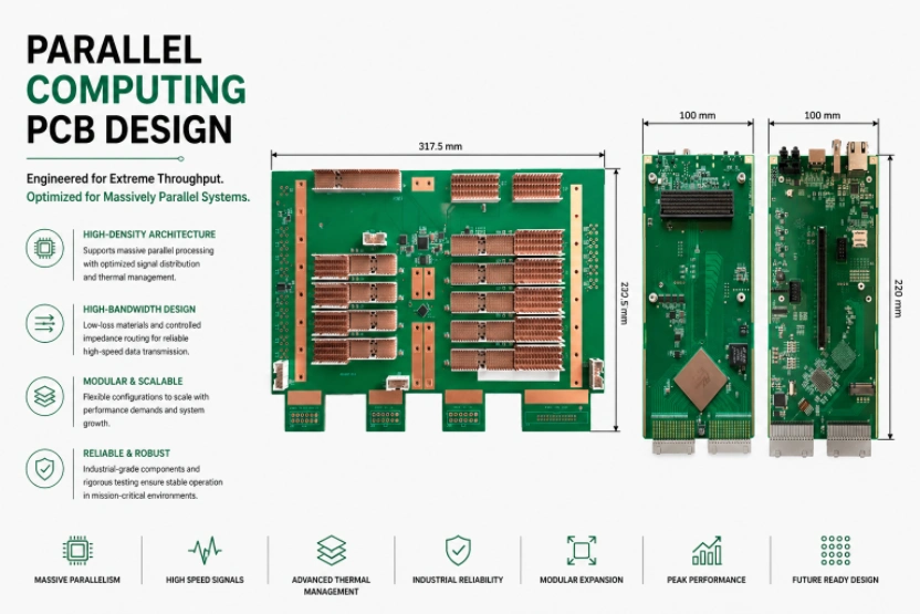
A current-generation GPU accelerator concentrates 700W of power, 3.35 TB/s HBM3e memory bandwidth, and 128 lanes of PCIe Gen 5/CXL 2.0 onto a single PCB measuring approximately 267×112 mm. These demands compound across every design domain simultaneously — power delivery, signal integrity, thermal management, and mechanical stability all operate at their absolute physical limits with zero margin for fabrication variability.The technical challenge is not any single parameter in isolation — it is the interaction between them. Heavy copper planes required for 800 A power delivery create impedance discontinuities that interfere with adjacent 112G PAM4 signal routing. Thermal via arrays needed for heat extraction consume routing channels required for HBM3e escape. Multi-phase VRM inductor placement zones conflict with high-speed memory bus keepout areas. Solving these interactions requires coordinated multi-domain design review that few fabricators have the expertise to execute.
HILPCB's parallel computing PCB program addresses these compounding challenges through simultaneous power-signal-thermal co-design — identifying and resolving conflicts between power plane geometries, high-speed routing channels, and thermal via arrays before they reach fabrication.
Defining Challenges of Parallel Computing PCB Design
- Power Concentration: 800+ A at sub-0.75V core voltages with <5 mV ripple under 200 A/μs transients — requiring 16–24 phase VRMs with heavy copper planes (4–6 oz internal) that must not create impedance discontinuities for adjacent 112G signal routing.
- Memory Bandwidth at Substrate Limits: HBM3e interfaces at 9.6 Gbps per pin across 1024-bit buses, and GDDR7 at 36 Gbps per pin using PAM4 signaling — data rates where PCB dielectric loss and copper roughness are the primary bandwidth limiters, not silicon speed.
- Mechanical Stress Under Thermal Load: Board warpage below 0.3% of diagonal under sustained 700W thermal load — preventing TIM contact loss, BGA solder fatigue, and PCIe connector disengagement during multi-day training runs.
- Fabrication Complexity at Scale: 20–32 layers mixing sequential HDI lamination with through-hole vias, 4–6 oz heavy copper power planes, and 3/3 mil trace/space signal routing on ultra-low-loss dielectrics — yield challenges requiring fabrication expertise that eliminates the 30–40% scrap rate typical of less capable fabricators.
These demands make parallel computing PCBs among the most technically challenging commercial boards manufactured — and the most costly when fabrication quality falls short.
Power Delivery Architecture for 700W+ Accelerator Cards
Parallel hardware draws power levels rivaling industrial equipment — a training GPU pulls 700W continuously for days during large language model training, an FPGA array sustains 400W indefinitely during real-time video transcoding, and next-generation accelerators on the roadmap exceed 1000W per card. Clean power delivery at these levels determines whether the accelerator achieves its rated TFLOPS throughput or throttles under transient-induced voltage droop that can reduce training performance by 15–20%.The PDN design challenge is fundamentally different from standard server boards. A GPU die executing a matrix multiplication across all 16,384 cores creates current transients exceeding 200 A/μs — fast enough that even well-designed power planes exhibit voltage droop unless the PDN impedance profile is flat from DC through 500 MHz. This requires not just heavy copper, but precisely engineered plane geometries with decoupling placement validated through full-wave electromagnetic simulation.
PDN Engineering for Parallel Accelerators
- Multi-Phase VRM Layout: 16–24 phase buck converters with DrMOS power stages and inductors placed within 2 mm of IC power balls. Phase current loops routed on heavy copper layers (4–6 oz internal, 6–10 oz external on dedicated power modules) maintaining loop inductance below 80 pH per phase.
- Power Plane Partitioning on Dedicated Layers: Separate, uninterrupted copper planes for core voltage (0.65–0.85V), HBM I/O (1.05V), SerDes (0.9V), and auxiliary rails — each on dedicated multilayer planes with no signal via penetrations. Anti-pad geometries around signal vias optimized through 3D field solver to prevent localized impedance spikes in power planes.
- Distributed Decoupling by Impedance Target: 400–800 capacitors placed by full-wave PDN impedance simulation — not rule-of-thumb placement — maintaining PDN impedance below 0.5 mΩ from DC through 500 MHz. Via connections from capacitor pads to power/ground planes use via-in-pad with back-drilled stubs to minimize ESL contribution.
- Real-Time Current Telemetry: High-precision shunt resistor networks (±0.5% tolerance, 4-terminal Kelvin connection) on each major rail providing real-time power measurement at ±1% accuracy — integrated with datacenter infrastructure management through PMBus/I²C for GPU power capping and thermal throttling coordination.
Validated Power Integrity Process
Every accelerator board undergoes PDN impedance measurement using vector network analyzer (VNA) from 100 Hz to 1 GHz — verifying that the fabricated board meets the simulated target impedance profile across all frequency decades. Boards failing the impedance mask are rejected before component assembly, preventing the costly discovery of power integrity issues during system integration.
HBM3e and GDDR7 Memory Interface Routing
Parallel processors achieve their throughput by accessing memory across extremely wide, extremely fast buses. HBM3e uses 1024-bit interfaces at 9.6 Gbps per pin delivering 1.2 TB/s per stack (4.8 TB/s across four stacks); GDDR7 uses 256-bit buses at 36 Gbps per pin using PAM4 signaling. These next-generation memory interfaces define the board's layer count, material system, and fabrication process complexity — and push organic PCB substrates to their fundamental physical limits.At these data rates, the PCB is not a passive interconnect — it is an active contributor to the memory channel's bit error rate. Dielectric loss (Df), copper surface roughness (Rz), and via stub resonance each contribute measurable degradation to eye opening. A fabrication process producing Df variation of ±0.001 at 15 GHz — well within standard tolerance — can shift GDDR7 eye margin by ±15%, potentially crossing the JEDEC compliance boundary.
Memory Routing Techniques for Next-Generation Interfaces
- HBM3e Interposer Integration: 2000+ BGA balls at 0.55 mm pitch — tighter than previous HBM generations — requiring HDI construction with sequential lamination, stacked microvias (0.075 mm laser-drilled), and 2/2 mil trace/space for escape routing. Via-in-pad with copper fill and planarization mandatory for this ball density.
- GDDR7 PAM4 Signal Integrity: PAM4 signaling at 36 Gbps demands insertion loss below 2.5 dB at 18 GHz Nyquist — requiring ultra-low-loss laminates (Dk 3.0, Df 0.0015 at 10 GHz, such as Panasonic Megtron 7 or Isola I-Speed) with HVLP copper foil (Rz < 1.5 μm) and impedance-controlled differential pairs length-matched within ±0.5 mil per byte group.
- Pre-Route Channel Simulation: Full S-parameter channel models extracted from the proposed stackup using 3D electromagnetic field solvers (not 2D approximations) verify eye opening against JEDEC mask requirements at worst-case process corners (max Df, max copper roughness, min/max dielectric thickness) before layout commitment.
- Crosstalk Management at PAM4 Voltage Levels: PAM4's three eye openings are each one-third the amplitude of NRZ — making crosstalk tolerance 9.5 dB tighter than NRZ for equivalent BER. Post-layout extraction confirms near-end and far-end coupling between adjacent GDDR7 channels stays below -35 dB, preventing data-dependent jitter that closes the already-narrow PAM4 eye margins.
PCIe Gen 5/Gen 6 and CXL Interconnect Signal Integrity
Accelerators communicate with host processors through PCIe Gen 5 at 32 GT/s, with Gen 6 at 64 GT/s and CXL 3.0 emerging on next-generation platforms. Each generation halves the insertion loss budget and doubles the sensitivity to impedance discontinuities — making the PCB channel the performance-limiting element that determines whether the system achieves theoretical peak throughput or falls back to lower link speeds.PCIe Gen 6 introduces PAM4 signaling to the PCIe standard for the first time, reducing the channel loss budget to approximately 20 dB — of which the PCB must consume no more than 6–8 dB including all via transitions, AC coupling capacitor discontinuities, and connector interfaces. At 32 GHz Nyquist frequency, every design decision matters: a suboptimal via-to-stripline transition adds 1–2 dB, and four such transitions in a typical channel consume half the PCB loss allocation.
PCIe Gen 5/6 Channel Optimization
- Loss Budget Allocation: Gen 5 allocates ~28 dB total channel loss with PCB portion below 8–10 dB. Gen 6 tightens to ~20 dB total with PCB below 6–8 dB — requiring via stub elimination (back-drilling to <6 mil residual), ultra-low-loss dielectric (Df < 0.002 at 15 GHz), and HVLP copper on all signal layers.
- Via Transition Engineering: Each layer transition adds 0.5–2.0 dB at 16–32 GHz depending on via geometry. Back-drilled through-holes, blind/buried vias, and optimized via-to-trace anti-pad geometries are modeled individually through 3D electromagnetic simulation and verified through TDR measurement on production boards.
- CXL Memory Expansion Support: CXL 2.0/3.0 links sharing the PCIe physical layer but requiring tighter jitter tolerance — CXL's cache-coherency protocol is less tolerant of retransmission latency than PCIe's posted write model, making signal integrity margin critical for CXL-attached memory pooling architectures.
- Eye Diagram Compliance Verification: First-article boards undergo eye diagram measurement at 32 GT/s (Gen 5) and 64 GT/s (Gen 6) using calibrated BERT and oscilloscope — confirming production channel meets compliance mask with documented margin. Eye measurements are performed at operating temperature, not room temperature only.
Sustained Full-Load Thermal Architecture
Parallel computing boards operate at maximum power for hours or days — LLM training runs execute for weeks, rendering jobs sustain peak GPU utilization for hours, and scientific simulations run until convergence. The thermal design must handle sustained full load at rated ambient (35–45°C datacenter inlet) without throttling or degrading component lifetime below the 5-year datacenter replacement cycle.The thermal challenge on parallel computing PCBs is not simply total power dissipation — it is power density. A 700W GPU die measures approximately 800 mm², concentrating over 87 W/cm² at the die surface. The PCB must conduct this heat through the package substrate, across the TIM interface, and into the heatsink or cold plate — and any gap, void, or warpage in this thermal path creates a hot spot that triggers localized throttling and reduces aggregate compute throughput.
Sustained-Load Thermal Design
- Processor Thermal Via Architecture: Dense thermal via arrays (0.3 mm diameter, 1.0 mm pitch) beneath GPU/FPGA packages connecting top-side BGA pad field to bottom-side copper pour interfacing with heatsinks through TIM. Via fill (copper or conductive epoxy) and surface planarization to ±10 μm ensure consistent TIM contact across the entire package footprint.
- VRM Thermal Management: 16–24 inductor phases each dissipating 2–4W create distributed heat sources totaling 30–60W of VRM loss. Component placement zoning keeps VRM components on the opposite board edge from temperature-sensitive clock oscillators, voltage references, and I²C sensors — maintaining ≥15 mm thermal separation.
- Warpage Control Under Thermal Load: Board warpage below 0.3% of diagonal through symmetric copper distribution across all layers, balanced lamination sequence, and CTE-matched prepreg/core selection — preventing TIM contact loss that reduces thermal conductivity by 3–5× at the separation point.
- Internal Heat Spreading: 3–4 oz copper inner planes spread heat laterally from concentrated die footprints, reducing peak-to-average temperature differential across the package mounting zone. Thermal simulation verified against IR thermography measurements on first articles under sustained load.
DFM for 20–32 Layer Accelerator Board Fabrication
Parallel computing PCBs are among the most complex commercial boards manufactured — 20–32 layers mixing sequential HDI lamination with through-hole vias, heavy copper power planes alongside fine-line signal routing, and ultra-low-loss materials that require specialized lamination profiles. Manufacturing yield depends entirely on DFM discipline applied during design — and on fabricator capability validated through statistical process data, not marketing claims.HILPCB's fabrication capability extends to 64 layers for the most demanding constructions, with production-validated processes for 28–32 layer accelerator boards achieving >92% first-pass yield. Our DFM review for parallel computing boards identifies the fabrication risk interactions that standard automated design rule checks miss — the coupling between heavy copper warpage forces, sequential lamination registration drift, back-drill positional accuracy, and ultra-low-loss material lamination temperature sensitivity.
DFM Process for Complex Accelerator Boards
- Sequential Lamination Registration: ±1.5 mil layer-to-layer accuracy across 20–32 layer sequential builds verified through X-ray alignment target measurement at each lamination cycle — preventing via-to-pad misalignment on 0.55 mm pitch HBM BGA escape routes where a 2 mil shift causes an open circuit.
- Back-Drill Depth Control: Via stubs controlled to <6 mil through laser-registered back-drilling with in-process depth verification using cross-section measurement every 50th panel — each mil of excess stub creates a quarter-wave resonance that produces a notch in the channel frequency response.
- Copper Balance Analysis: Heavy copper power layer distribution (4–6 oz) analyzed for bow/twist using finite element modeling — asymmetric copper creates warpage exceeding 0.5% that impacts both component placement accuracy and thermal interface contact.
- Material Compatibility Validation: Mixed material stackups (ultra-low-loss signal layers with standard FR-4 power layers) validated for lamination compatibility — CTE mismatch between dissimilar materials causes inter-layer stress that can produce delamination during thermal cycling.
- Prototype Validation: First articles with full electrical verification (TDR, VNA, eye diagrams), cross-section analysis, and thermal characterization before production tooling commitment — critical when a respin costs $80K+ and 8–10 weeks of schedule impact.
HILPCB Parallel Computing PCB Manufacturing
HILPCB manufactures parallel computing PCBs for GPU accelerator OEMs, FPGA integrators, AI training infrastructure companies, and datacenter operators across North America, Europe, and Asia-Pacific.Our fabrication capabilities for parallel computing boards include up to 64-layer sequential HDI lamination with ±1.5 mil registration, 4–6 oz heavy copper power planes with multi-phase VRM routing supporting 800+ A delivery, ultra-low-loss dielectrics (Df < 0.002 at 15 GHz) for PCIe Gen 5/6, CXL, and GDDR7, HBM3e interposer support with 0.55 mm pitch BGA escape routing at 2/2 mil trace/space, warpage control below 0.3% under sustained thermal load, and IPC-6012 Class 3 fabrication with full lot traceability and VNA-verified PDN impedance on every production board.
Whether you're developing the next-generation GPU accelerator or scaling AI training infrastructure, our engineering team works alongside your design group from stackup definition through production ramp — ensuring that fabrication capability is validated before layout commitment, not discovered during first-article testing.
Parallel Computing PCB FAQ
How do parallel computing PCBs handle 800A power delivery?
Delivering 800+ Amps requires heavy copper inner planes (4-6 oz) and 16-24 phase VRMs placed as close to the processor as possible. The power delivery network (PDN) must be designed using full-wave 3D electromagnetic simulation to keep impedance below 0.5 mΩ up to 500 MHz, preventing transient voltage droop.
Why is via stub length critical for 112G PAM4 signals?
At 112G PAM4 (56 GHz Nyquist), via stubs act as resonant antennas that absorb signal energy, creating severe notches in the channel's frequency response. Back-drilling to leave a residual stub of <6 mils is mandatory to preserve the tight PAM4 eye diagram.
What causes board warpage in GPU accelerator cards?
Warpage is primarily caused by asymmetric copper distribution, especially the thick copper layers used for high current, combined with the extreme heat cycling of 700W workloads. We control warpage to <0.3% using perfectly balanced stackups, symmetric copper pours, and CTE-matched materials.
Request engineering review for your accelerator board program →