
When a PCB fabricator's CAM engineer asks for permission to "add copper thieving for plating balance," replying with a blanket "Approved" without inspecting the returned Gerber overlay is one of the fastest ways to detune an RF antenna, shift outer-layer microstrip impedance, or violate a high-voltage creepage barrier. Conversely, rejecting all copper additions outright can leave isolated outer-layer traces and via barrels vulnerable to severe electroplating thickness variations and etch undercut.
Making the right engineering call requires separating three concepts that fabrication notes frequently conflate—galvanic copper thieving, lamination copper balancing, and functional grounded copper pours—and auditing the proposed CAM geometry zone by zone against your board's electrical keepouts. For broader stackup symmetry and heavy-copper thermal planning, see our high-current copper balancing guide.
1. The Galvanic Physics: Why Isolated Traces Over-Plate Without Thieving
During outer-layer pattern plating, the drilled and copper-seeded manufacturing panel is submerged in an electrolytic bath and connected as the electrical cathode. Photoresist covers the background areas that will later be etched away, leaving only the desired traces, pads, and through-hole barrels exposed to receive electrolytic copper (followed by tin etch-resist).
As explained in published galvanic process documentation, electroplating current does not distribute evenly across a panel when copper density varies sharply from region to region:
- High Local Current Density on Isolated Features: Electric field lines crowd onto isolated copper traces or lone connector pads surrounded by large expanses of bare dielectric (photoresist). Because local deposition rate scales with local current density (J), isolated features attract disproportionately thick copper and tin plating.
- Mushrooming, Etch Undercut, and Mask Thinning: When copper plates above the height of the dry-film photoresist walls, it spreads laterally ("mushrooming"). During subsequent etching, thick copper requires longer dwell times, causing lateral undercut on fine-pitch traces. Excessively tall isolated traces can also exceed target conductor height and suffer thin solder-mask coverage over sharp top corners.
- Starved Current in Dense Zones: Meanwhile, high-density BGA or bus routing zones with large exposed copper surface area share the local current across many conductors, risking lower hole-wall barrel copper thickness (PTH < 20 μm) unless total bath current or cycle time is increased.
Adding copper thieving (non-functional, isolated sacrificial copper dots, squares, or hatching—often called "robber bars" on panel rails) increases the exposed cathode surface area in sparse zones. It "robs" excess current density away from isolated signal traces so the entire panel plates within a tight copper thickness window. Fabricators often evaluate this distribution before release using a density map such as published plating-index metrics.
2. Separating Three Commonly Conflated Requests
Because different design guides and CAM shops use "thieving" and "balancing" interchangeably, always classify a supplier proposal by layer, mechanical/electrical function, and net connectivity rather than by its email label:
| Engineering Term | Primary Manufacturing Mechanism | Typical Layer & Location | Electrical Connectivity State | Who Must Approve Changes |
|---|---|---|---|---|
| Galvanic Copper Thieving (Robber Patterns) | Equalizes cathode current density (J) during electrolytic pattern plating of outer layers and PTH barrels | Outer layers (Top / Bottom), placed on breakaway panel rails or open in-board areas | Electrically floating (isolated) small dots/squares; no net connection | CAM allowed on waste rails per order agreement; Design Owner must approve any in-board additions |
| Lamination Copper Balancing | Equalizes copper area across X/Y regions and symmetric layer pairs so prepreg resin flows evenly without resin starvation or bow/twist (copper distribution guidelines) | Inner layers (and outer layers); open mechanical areas or unused core regions | Usually floating hatch/dots (or tied to a reference plane only if designed in CAD) | Design + Stackup Owner (affects pressed dielectric thickness adjacent to controlled-impedance layers) |
| Functional Grounded Copper Pour | Provides low-inductance return path, coplanar waveguide (CPWG) shielding, or heat spreading | Any signal or plane layer within the finished PCB outline | Connected to GND (or power net) and stitched with vias | Strictly Design Owner — this is a circuit schematic/layout change, never routine CAM thieving |
Never allow a CAM engineer to tie newly added copper balance pours to GND under the label of "thieving." Connecting a copper pour to ground changes reference-plane capacitance, alters return-current loops, and creates resonant stubs if left unstitched at high frequencies.
3. Worked CAM Overlay Audit: Approve One Zone, Reject Another, Hold the Third
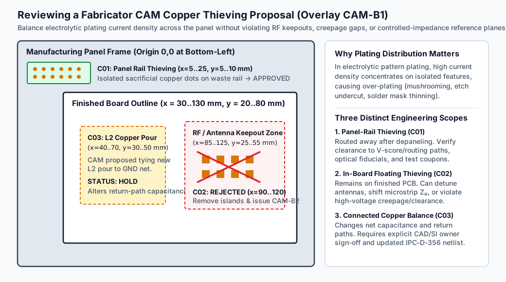
To see how a zone-by-zone CAM review works in practice, examine the downloadable review dataset (DEMO-B, incoming proposal CAM-B1) where the finished PCB occupies panel coordinates x = 30..130 mm, y = 20..80 mm, and the design drawing defines a restricted RF / Antenna No-Addition Keepout at x = 85..125 mm, y = 25..55 mm:
| Request ID | Layer & Panel Coordinates | Proposed Feature & Electrical State | Stated CAM Rationale | Design Constraint Checked | Engineering Decision & Action |
|---|---|---|---|---|---|
| C01 | Top Layer (CAM-B1)x = 5..25 mm, y = 5..10 mm |
Isolated copper dot array on breakaway panel rail | Balance outer-layer plating current near sparse board edge | Outside product outline (x = 30..130 mm); clears fiducials, tooling holes, and V-score line |
APPROVE WITH SCOPE — Permitted on waste rail only; routed off before shipment |
| C02 | Top Layer (CAM-B1)x = 90..120 mm, y = 30..50 mm |
Isolated floating copper squares inside finished board | Fill open top-layer region to improve local plating uniformity | Overlaps RF Keepout Zone (x = 85..125, y = 25..55 mm) near antenna / RF launch |
REJECT REGION — Floating metal islands detune antenna radiation and couple parasitically; strip C02 |
| C03 | Inner Layer L2 (CAM-B1)x = 40..70 mm, y = 30..50 mm |
Solid copper pour connected to GND net inside board |
Improve L2 lamination resin balance and Z-axis symmetry | Unapproved electrical net modification; alters L1/L3 reference capacitance | HOLD FOR DESIGN — Do not approve as CAM thieving; evaluate non-connected cross-hatch or stackup adjustment |
| C04 | Top Layer (CAM-B2)x = 5..25 mm, y = 5..10 mm |
Revised overlay returning only C01 rail pattern (C02/C03 removed) |
Close EQ from CAM-B1 review |
Diff CAM-B2 Gerber layers against original DEMO-B + C01 boundary |
VERIFY & RELEASE — Confirm C02 and C03 are 100% absent in CAM-B2 before releasing to photoplot |
(Downloadable CAM approval log and alternative matrix: bounded-cam-approval.csv, manufacturing-alternatives.csv, and notes.)
Notice why Step C04 is mandatory: approving C01 while rejecting C02 and C03 on CAM-B1 is a conditional instruction, not a final sign-off. The engineer must visually diff the revised CAM-B2 Gerber overlay against the released DEMO-B artwork to verify that all rejected islands were actually deleted before authorizing production.
4. Six Protected Zones Where In-Board Thieving Must Be Excluded
When reviewing a proposed in-board thieving overlay, verify clearances against these six functional zones:
- Chip/PCB Antennas, Baluns, and RF Launches: Floating copper islands placed under or near an inverted-F antenna, patch antenna, or RF connector launch act as parasitic directors/resonators, shifting resonant frequency and degrading return loss (S11).
- Controlled-Impedance Microstrip and Stripline Channels: Adding thieving dots near the edge of a surface microstrip trace—or adding copper balance hatching on an adjacent reference layer—changes fringe capacitance and shifts characteristic impedance (Z0). Keep thieving outside the agreed 3H--5H lateral clearance envelope of controlled-impedance nets.
- High-Voltage Creepage and Clearance Barriers: Floating conductive islands placed across an isolation slot, optocoupler/transformer barrier, or primary-to-secondary mains boundary reduce the effective creepage/clearance distance (the floating islands act as intermediate stepping stones for arc tracking).
- Optical Fiducials and Alignment Targets: Keep a clean, unpopulated copper-free keepout ring around global and local SMT fiducials so pick-and-place machine vision never confuses a thieving dot with the fiducial mark (see our PCB fiducial marks guide).
- Depaneling Paths (V-Score, Mouse Bites, and Router Channels): Copper thieving placed directly across a V-score groove or router path smears against cutter blades, creates metallic burrs, and risks edge delaminations during depaneling.
- Exposed Mechanical / Shield Grounding Lands: Ensure thieving patterns do not encroach on chassis mounting pads, EMI shield cans, or optical sensor windows.
5. Manufacturing Alternatives When In-Board Thieving Is Prohibited
If your board is an RF module, high-voltage power supply, or dense sensor where in-board copper additions are strictly forbidden, ask the fabricator to evaluate process-side alternatives:
| Manufacturing Alternative | How It Solves the Distribution Problem | Commercial & Process Impact to Confirm |
|---|---|---|
Wider Panel-Rail Robber Bars (C01) |
Places sacrificial copper frames and dot grids immediately outside the board outline on waste rails (panel preparation guide) | Zero impact on finished PCB electrical behavior; may slightly increase rail width on the production panel |
| Modified Panel Stepping / Orientation | Rotates alternating boards 180° on the production panel so sparse edges sit adjacent to denser copper zones | Preserves board artwork unchanged; confirm assembly conveyor orientation if shipping in multi-up arrays |
| Pulse / Adjusted Current-Density Plating | Uses lower average current density with longer bath dwell time or periodic pulse-reverse plating waveforms | Improves throwing power and surface uniformity without in-board copper edits; confirm capability and schedule |
| CAD-Controlled Cross-Hatch Reference Pour | Layout engineer adds a deterministic, simulated pour or keepout-compliant balance grid in native CAD and re-exports Gerbers | Keeps master CAD, IPC-D-356 netlist, and SI field-solver models 100% synchronized across future revisions |
6. How to Specify Copper Thieving Rules in Fabrication Notes
Instead of leaving thieving permissions ambiguous, place an explicit, bounded instruction in your fabrication drawing notes (and align it with your Gerber data preparation manifest):
CAM Copper Thieving & Balancing Note:
- Fabricator may add non-functional copper thieving / galvanic robber patterns outside the finished board outline on breakaway panel rails, maintaining ≥ 1.0 mm clearance to board profile, V-score/routing paths, tooling holes, and panel fiducials.
- Do not add copper thieving, balancing grids, or connected pours inside the finished board outline without submitting a marked layer-by-layer Gerber overlay for written engineering approval.
- Strictly preserve all copper keepout zones defined on mechanical/keepout layers (including RF antenna regions, high-voltage isolation barriers, and controlled-impedance channels).
HILPCB's CAM engineering team reviews every multilayer PCB, HDI PCB, and Rogers RF PCB submission for plating current distribution and lamination copper balance before release. When copper compensation is recommended inside the board outline, we issue a clear before/after Gerber overlay via an Engineering Query (EQ) so your hardware team retains full control over RF, high-speed, and safety-isolation zones. Upload your design package to request a quote and start your DFM review.
Frequently Asked Questions
What is the difference between copper thieving and copper balancing?
Copper thieving specifically refers to non-functional copper dots, squares, or rail strips added to outer layers to equalize cathode current density during electrolytic copper plating, preventing isolated traces from over-plating. Copper balancing is the broader practice of equalizing copper coverage across a layer and between symmetric layers in the stackup so prepreg resin fills uniformly during lamination and the finished board resists bow and twist.
Can floating copper thieving dots affect RF or high-speed signal integrity?
Yes. Even though floating thieving dots are not wired to any schematic net, they introduce parasitic capacitance and eddy-current coupling when placed near high-speed microstrip/stripline edges, differential pairs, inductors, or antennas. Always define explicit CAD keepout zones around RF launches, antennas, and controlled-impedance channels.
Why does copper thieving use small grid dots or squares instead of a solid copper plane?
In outer-layer plating, small evenly spaced dots or squares allow the CAM system to tune local copper area percentage smoothly without creating a large solid plane that could trap laminating gases, blister during reflow thermal shock, or act as a large unintended capacitive plate. On inner layers, vented cross-hatch or dot patterns also allow prepreg resin to bond directly to the underlying core laminate through the openings, improving interlaminar peel strength.
Should I let the fabricator add thieving in CAM, or add it myself in my CAD layout?
Allow the fabricator's CAM team to place galvanic thieving on panel waste rails, since rail layout depends on the factory's specific panel size and plating rack geometry. For any copper balancing required inside the finished board outline on RF, high-speed, or high-voltage boards, either generate the keepout-bounded pattern directly in your CAD tool or require a formal CAM Gerber overlay approval so your master design files never diverge from the manufactured board.