Your PCB looks perfect in the CAD software. Simulations pass. Component selections check out. Then manufacturing sends it back red-marked with violations, or worse - boards manufacture fine but fail during testing. These problems waste weeks and thousands in rework. Professional engineering catches issues before they become expensive disasters.
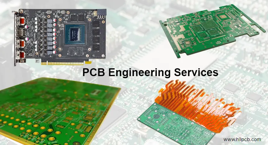
HILPCB engineering services bridge the gap between electrical design and manufacturing reality, optimizing for performance, manufacturability, and cost simultaneously.
Why PCB Designs Fail Without Engineering Review
Most design failures trace back to the same root causes. Designers optimize for functionality but miss manufacturing constraints. CAD tools flag basic violations but can't catch context-specific problems. Nobody validates that the design actually works in the real world until it's too late to fix easily.
The Common Failure Points
Manufacturing rejects designs for trace-space violations, insufficient annular rings, or solder mask problems that standard design rule checks miss. High-speed signals fail compliance testing because impedance calculations ignored manufacturing tolerances. Components overheat because thermal management got an afterthought. Board dimensions don't fit enclosures because mechanical coordination never happened.
Engineering review during design phase catches these issues when fixes are simple. After boards manufacture, rework costs 10-50× more than preventing problems upfront. Our team reviews designs within 24 hours, identifying critical issues that need immediate attention versus optimizations that improve cost or performance.
DFM Analysis That Actually Prevents Manufacturing Problems
Adding "DFM check" to your order doesn't guarantee manufacturability. Understanding what manufacturers actually check - and what they skip - helps you specify meaningful requirements that prevent production delays.
What Standard DFM Checks Miss
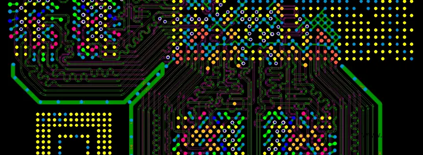
Most automated DFM tools verify basic spacing rules and flag obvious violations. They miss context-specific problems that cause real production failures. A 6mil trace spacing might pass automated checks but cause yield problems on outer layers due to etching variation. Annular rings that look adequate on screen break during drilling when tolerance stack-up gets factored in.
Comprehensive DFM Review Includes
- Trace geometry analysis accounting for layer-specific manufacturing capabilities (outer layers: 6/6mil, inner layers: 4/4mil minimum)
- Annular ring calculations including drilling tolerances, registration accuracy, and plating thickness variations
- Via aspect ratio verification to prevent plating failures (10:1 maximum for through-holes, HDI microvias for tighter designs)
- Solder mask design review ensuring no slivers under 4mil that break off during processing
- Panel optimization analysis showing how board dimensions affect cost per unit
- Material compatibility verification for special requirements like RF designs or high-temperature applications
Our engineers review against actual PCB manufacturing capabilities from our facility, not generic textbook rules. We explain why violations matter and provide specific corrections, not just "fix this" without context.
The Panel Optimization Opportunity
Standard panels measure 18×24 inches. Designs slightly over half-panel size waste expensive space - a 13-inch board length versus 12-inch means half as many boards per panel, doubling cost. Small dimensional adjustments often yield dramatic savings. We analyze your board dimensions and suggest optimizations that balance size requirements with manufacturing efficiency.
High-Speed Design Issues You Can't See Until Testing
Signal integrity problems don't show up until boards undergo compliance testing or field trials. By then, fixing requires complete redesign. Engineering analysis during design phase identifies problems through simulation before hardware exists.
When Signal Integrity Engineering Becomes Critical
Digital signals above 100MHz behave as transmission lines where PCB geometry determines success or failure. USB 3.0 at 5Gbps, HDMI, Ethernet, and PCIe all require impedance control and proper return path management. Get it wrong and signals reflect, creating timing violations and bit errors.
The Impedance Control Reality
Specifying "50-ohm traces" doesn't make them 50 ohms. Actual impedance depends on trace width, dielectric thickness, copper weight, and material properties - all subject to manufacturing variation. Designs must account for tolerances to ensure actual impedance stays within specification limits (typically ±10%).
We calculate exact trace geometry based on your stackup and account for:
- Copper plating thickness variation (±0.3mil typical)
- Dielectric constant tolerance (±10% for standard FR4)
- Dielectric thickness variation (±10% for prepreg, ±5% for core)
- Trace width etching variation (±1mil)
Impedance testing during PCB fabrication verifies actual values. Without proper design accounting for tolerances, test results often fall outside specifications.
Differential Pair Routing Requirements
USB, HDMI, and other differential interfaces need constant spacing and tight length matching. Spacing determines differential impedance while length mismatch creates skew between positive and negative signals. Requirements vary by interface:
- USB 3.0: 90Ω ±10%, <0.5mm length mismatch
- HDMI: 100Ω ±10%, <0.25mm length mismatch
- PCIe Gen3: 85Ω ±10%, <0.3mm length mismatch
- Ethernet 1000Base-T: 100Ω ±10%, <0.5mm length mismatch
We provide routing guidelines specific to your stackup and signal requirements, coordinating with PCB design implementation.
Thermal Management Before Components Start Failing
Power dissipation creates heat. Without proper thermal design, components exceed temperature ratings and fail - sometimes during initial testing, often after weeks in the field when warranty costs multiply.
Thermal Design Starts With Power Budget
Calculate power dissipation for every component generating significant heat. Processors, power semiconductors, high-current traces all need thermal analysis. Junction temperature must stay below maximum ratings with adequate margin for reliability.
Thermal Via Arrays Extract Heat
Heat generated in component package must transfer somewhere. Thermal vias beneath thermal pads provide low-resistance paths to internal copper planes or opposite-side heat sinks. Via count and placement determine thermal resistance.
For power devices dissipating 2-5W, we typically specify:
- 20-30 thermal vias, 12mil diameter
- Placed directly under thermal pad in array pattern
- Spacing prevents solder wicking during PCB assembly reflow
- Connected to large copper area for heat spreading
Heavy Copper for High-Current Applications
Standard 1oz copper handles ~1A per mm width before exceeding acceptable temperature rise. Power supplies and motor drives often need 5-20A, requiring 2oz, 3oz, or heavier copper. We calculate required trace widths based on current levels, ambient temperature, and acceptable temperature rise, then specify appropriate copper weights.
Engineering Process and Deliverables
Engineering support starts with design file review. We accept all major formats - Altium, Cadence, KiCAD, Eagle, or Gerber files. Native design files enable most thorough analysis but we work with whatever you have.
24-Hour Standard Review Includes
- Complete DFM analysis with marked-up drawings showing specific issues
- Impedance verification for controlled impedance designs
- Thermal assessment flagging potential problem areas
- Cost optimization recommendations
- Clear explanations of why issues matter and how to fix them
Complex designs requiring detailed signal integrity simulation or thermal modeling take 2-3 days. We provide preliminary feedback immediately for schedule-critical items.
Extended Engineering Services
Beyond standard DFM review, we offer:
- Signal integrity simulation and optimization
- Thermal modeling and heat sink sizing
- Power distribution network analysis
- Layer stackup design and optimization
- Component selection and availability review
- Design-for-test consultation
Our engineers work as extension of your team, providing specialized expertise without overhead of full-time staff. From prototype through production, we support your success. Visit www.hilpcb.com/en/ to discuss your engineering needs.