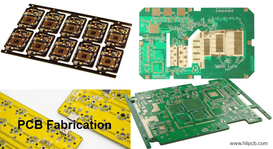
Modern electronics demand circuit boards that didn't exist five years ago. Smartphones pack more computing power than laptops into 6mm-thick bodies. 5G base stations transmit at 28GHz frequencies where FR4 becomes a signal killer. Automotive radar needs to see 300 meters ahead while surviving under-hood temperatures and vibration. These aren't academic challenges—they're daily requirements for PCB fabrication in 2025.
The gap between "can fabricate PCBs" and "can fabricate these PCBs" defines product success. HILPCB specializes in the challenging boards: any-layer HDI for wearables under 0.4mm thick, Rogers RT/duroid for 77GHz automotive radar, rigid-flex for medical implants, and back-drilled boards for 56Gbps SerDes links.
HDI Fabrication for Ultra-Compact Devices
The Miniaturization Challenge
Flagship smartphones now pack 12+ cameras, 5G modems, wireless charging, and 5000mAh batteries into bodies under 8mm thick. Component density reached physical limits of standard through-hole vias years ago. The solution: High-Density Interconnect (HDI) with laser-drilled microvias connecting only adjacent layers.
HDI Capabilities:
- Any-layer microvia structures (1+N+1 to 4+N+4 build-up)
- Laser drilling: 50-150µm diameter microvias
- Line/space: 2/2mil (50µm) minimum
- Sequential lamination for complex stackups
- Via-in-pad technology for BGA fanout
Applications:
- Smartphones & Tablets: Mainboards with 0402/0201 components, fine-pitch BGAs
- Wearables: Ultra-thin boards (0.4-0.6mm) with rigid-flex sections
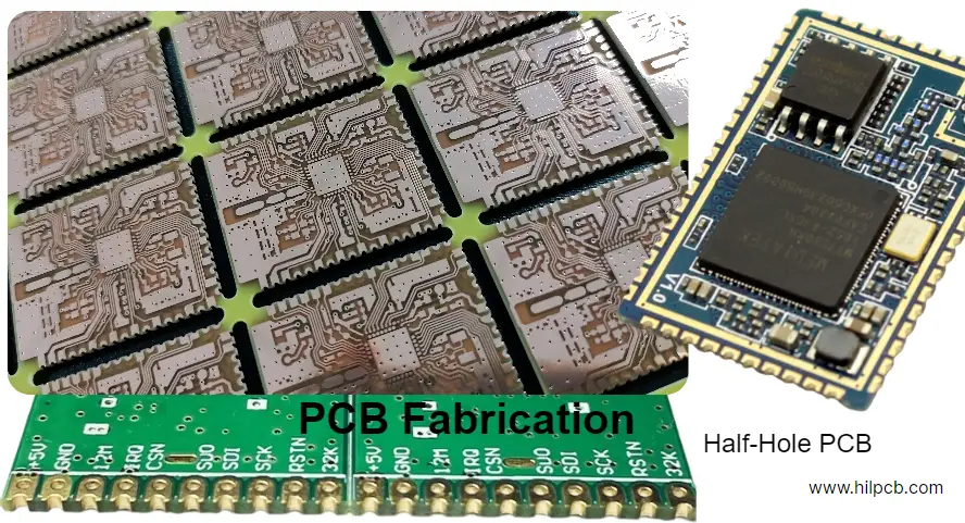
- True Wireless Earbuds: Miniature PCBs under 15mm x 8mm (see our earbuds PCB design guide)
- Medical Implants: Biocompatible polyimide HDI for pacemakers, neurostimulators
Why HDI vs Standard Multilayer? Standard 8-layer board with through-vias: 1.6mm thick, 50% routing efficiency. 8-layer HDI with microvias: 0.8mm thick, 85% routing efficiency, better signal integrity.
Cost premium: 40-80% over standard multilayer. Worth it when board area is constrained or fine-pitch BGAs (0.4mm pitch) are required.
Rogers & RF Material Fabrication for High-Frequency Systems
When FR4 Fails: The High-Frequency Problem
FR4 works fine at 1-2 GHz. At 10 GHz, signal loss becomes excessive. At 28 GHz (5G mmWave) or 77 GHz (automotive radar), FR4 is unusable. The dielectric loss tangent (Df) and frequency-dependent dielectric constant (Dk) cause signal degradation measured in dB per inch.
Rogers Material Solutions:
| Material | Frequency Range | Dielectric Constant (Dk) | Applications |
|---|---|---|---|
| RO4003C / RO4350B | 1-10 GHz | 3.38 / 3.48 | 5G sub-6GHz, WiFi 6E, automotive radar (24GHz) |
| RO4835 | 1-35 GHz | 3.48 | High-performance 5G, satellite |
| RT/duroid 5880 | 10-77 GHz | 2.20 | mmWave 5G (28/39GHz), automotive radar (77/79GHz) |
| RT/duroid 6002 | DC-77 GHz | 2.94 | Aerospace, military, temperature-stable |
Fabrication Challenges:
- Lower lamination temps: Rogers materials degrade above 200-220°C (FR4 uses 170-180°C)
- Specialized drilling: PTFE materials gum drill bits; requires unique parameters
- Impedance control: ±3Ω tolerance requires thickness measurement to ±5µm (learn more about impedance control)
- Hybrid stackups: Rogers outer layers + FR4 core reduces cost by 40-60%
Real Applications:
- 5G Base Stations: RO4350B for 3.5GHz massive MIMO antenna boards
- Automotive Radar: RT/duroid 5880 for 77GHz collision avoidance, adaptive cruise control
- Satellite Communications: RT/duroid 6002 for Ka-band (26.5-40 GHz) transponders
- WiFi 6E / 7: RO4003C for 6GHz band routers and access points
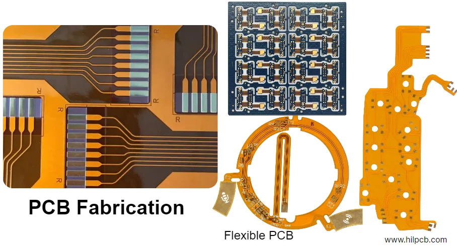
Rigid-Flex Fabrication for 3D Packaging
Why Rigid-Flex? When Connectors and Cables Fail
Connectors add cost, create failure points, and consume space. Ribbon cables wear out. For products requiring 3D board placement—medical devices, aerospace avionics, compact cameras, foldable phones—rigid-flex eliminates interconnect failures while enabling impossible form factors.
Rigid-Flex Structure:
- Rigid sections (FR4 or polyimide): Component mounting, structural support
- Flex sections (polyimide film): Dynamic bending, 3D routing, articulation
- Sequential lamination bonds rigid and flex in single structure
- Adhesiveless construction for better electrical performance and thinner profile
Construction Options:
- 2-20 total layers
- 1-4 flex layers per flex section
- Multiple flex zones in single board
- Controlled impedance through flex sections
- EMI shielding with copper-clad coverlay
Applications:
- Medical Implants: Pacemakers, cochlear implants, neurostimulators (biocompatible polyimide)
- Aerospace Avionics: Weight-critical applications, vibration resistance
- Foldable Phones: Display driver boards with dynamic flexing (200,000+ cycles)
- Drones: Weight reduction, compact motor controllers
- Military Wearables: Conformal antennas, body-worn systems
Cost Reality: Rigid-flex costs 2-4× standard rigid boards due to:
- Sequential lamination (multiple press cycles)
- Specialized tooling and fixturing
- Yield challenges in flex-to-rigid transition zones
- Material cost (polyimide 3-5× FR4)
Justified when eliminates connectors (cost + failure rate) or enables impossible form factors.
⚡ Quick Turn Fabrication Timelines
| Board Type | Specification | Lead Time |
|---|---|---|
| Standard Rigid | 2–6L FR4, standard stack-up | 24–48 hours |
| HDI | 1+N+1 / 2+N+2, laser microvias | 8–14 days |
| Rogers RF | RO4350B/4003C, controlled impedance | 7–12 days |
| Rigid-Flex | Up to 12 layers with flex zones | 15–25 days |
| Metal Core | Aluminum/copper base, thermal vias | 8–12 days |
*Expedited service available. Lead times may extend 3–7 days depending on material availability.
Metal Core & Thermal Management PCBs
The Heat Problem in Power Electronics
Power LEDs, IGBTs, SiC MOSFETs, and RF power amplifiers generate heat that standard FR4 cannot dissipate. Copper layers spread heat laterally, but thermal conductivity (0.3-0.4 W/mK for FR4) barely moves heat vertically to heatsinks. Metal core PCBs solve this with 10-1000× better thermal conductivity.
Metal Core PCB (MCPCB) Types:
| Core Material | Thermal Conductivity | Applications | Cost vs FR4 |
|---|---|---|---|
| Aluminum 5052 | 1-3 W/mK | LED lighting (residential, commercial) | 1.5-2× |
| Aluminum 6061 | 3-10 W/mK | High-power LEDs, motor drives | 2-3× |
| Copper C1100 | 200-400 W/mK | RF power amplifiers, EV inverters | 4-8× |
Structure:
- Circuit layer (copper traces, typically 1-4oz)
- Dielectric insulation layer (thermal interface, electrically isolating)
- Metal core base (aluminum or copper)
Fabrication Considerations:
- Dielectric thickness: 50-200µm (thinner = better thermal but harder to manufacture)
- Via technology: Thermal vias drilled through to metal core for maximum heat transfer (see thermal via design)
- No plated through-holes (core is grounded or thermally conductive, not electrical routing)
- CTE mismatch management between copper circuit and aluminum/copper core
Real Applications:
- High-Power LED Arrays: Street lighting, stadium lighting, automotive headlights
- EV Power Electronics: Motor controllers, DC-DC converters, charging systems
- RF Power Amplifiers: 5G massive MIMO base stations, broadcast transmitters
- Industrial Motor Drives: VFDs, servo drives with IGBTs or SiC devices
Advanced Fabrication Processes
Laser Direct Imaging (LDI) for Fine Features
Traditional photomask process hits resolution limits around 3/3mil (75µm) due to film distortion, contact exposure gaps, and alignment errors. Laser Direct Imaging projects patterns directly onto photoresist-coated panels with micron-level accuracy.
LDI Advantages:
- 2/2mil (50µm) lines reliably
- No film costs or storage
- Design changes in minutes, not hours
- ±25µm registration accuracy layer-to-layer
When LDI is Required:
- Fine-pitch BGAs (0.4-0.5mm pitch)
- HDI with dense microvias
- RF boards with narrow transmission lines (impedance control)
- Any board >12 layers (alignment criticality)
Back-Drilling for High-Speed Signals
Via stubs act as unterminated transmission line stubs, causing reflections at high frequencies. Critical for:
- PCIe Gen4/Gen5 (16/32 Gbps per lane)
- 25G/56G SerDes (server backplanes, switches) - see our backdrill PCB guide
- DDR5 memory interfaces
- High-speed digital >10 Gbps
Back-Drilling Process:
- Standard through-via drilled and plated
- From opposite side, controlled-depth drill removes unused stub
- Typical backdrill depth tolerance: ±75µm
- Leaves 100-150µm residual stub (vs 1-2mm without back-drilling)
Performance Impact:
- Return loss improvement: 5-10 dB at target frequency
- Extends usable bandwidth by 40-60%
- Eye diagram: cleaner with reduced jitter
Quality & Certifications
Testing & Inspection:
- AOI (Automated Optical Inspection) every layer
- X-ray for HDI microvias and layer registration
- Flying probe electrical testing (100% nets)
- TDR/VNA impedance testing (±3Ω tolerance verification)
- Microsection analysis for process validation
Certifications:
- ISO 9001:2015 (Quality Management)
- IATF 16949 (Automotive)
- ISO 13485 (Medical Devices)
- AS9100 (Aerospace)
- IPC-A-600 Class 2/3, IPC-6012 Class 2/3
- UL Listed, RoHS/REACH compliant
Why HILPCB for Advanced PCB Fabrication
We don't compete on price for simple 2-layer boards. Our expertise is the challenging fabrication: HDI for products under 1mm thick, Rogers materials for 28GHz 5G, rigid-flex for medical implants, back-drilled boards for 56G SerDes.
Technical Differentiators:
- Any-layer HDI up to 4+N+4 build-up
- Complete Rogers/Taconic/Arlon material line
- Rigid-flex up to 20 layers, multiple flex zones
- Back-drilling with ±50µm depth control
- Impedance testing every controlled impedance board
Engineering Support:
- Stackup design for signal integrity
- Material selection (performance vs cost tradeoffs)
- DFM analysis before tooling
- Impedance calculation and verification
- Thermal simulation for MCPCBs
Our comprehensive PCB prototyping service enables rapid iteration from concept to production, with the same manufacturing processes and quality standards throughout.
From 5nm chip packaging boards to 77GHz automotive radar, HILPCB fabricates the PCBs that define next-generation products.
FAQ
Q: When do I need HDI instead of standard multilayer? A: When component density requires via-in-pad for fine-pitch BGAs (≤0.5mm pitch), board thickness must be <1mm, or routing density exceeds 70% on standard multilayer. Cost premium: 40-80%.
Q: Rogers vs FR4 for 5G boards? A: FR4 works for sub-6GHz 5G. Rogers RO4350B required for good performance 6-10 GHz. RT/duroid 5880 mandatory for mmWave (24-39 GHz). Hybrid Rogers/FR4 stackups cut cost 40-60% vs full Rogers.
Q: What's the cost difference for rigid-flex vs separate boards + connectors? A: Rigid-flex 2-4× higher PCB cost. But eliminates connectors ($2-20 each), cables, assembly labor, and failure points. Break-even typically 5-10K units depending on connector count.
Q: Can you handle automotive (IATF 16949) and medical (ISO 13485)? A: Yes, both certified. Provide PPAP documentation for automotive, design history file (DHF) support for medical. Request certificate copies.
Q: What's included in DFM analysis? A: Trace width/spacing verification, drill size feasibility, copper balance check, impedance calculation, via aspect ratio analysis, material compatibility review. Free with quote.