Your prototype works beautifully. Customer validation complete. Orders coming in. Now you need 500 boards next month, 2,000 the month after, and 5,000 monthly by Q4.
Prototype success doesn't guarantee production success. Scaling requires different processes, different economics, different quality systems. Hand-built prototypes don't translate directly to automated manufacturing.
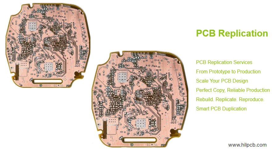
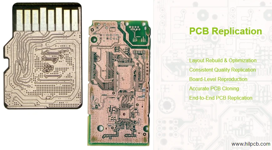
PCB replication transforms proven designs into cost-effective volume production through manufacturing optimization, supply chain management, and systematic quality control.
The Prototype-to-Production Gap (Why Direct Scaling Fails)
Most product teams encounter surprises scaling from prototype to production. Understanding why prevents costly mistakes:
Prototype Reality vs Production Reality:
Your prototype received special treatment. Experienced technician hand-assembled it carefully. Components cherry-picked from inventory. Extra time for rework and adjustments. Testing under ideal conditions. Result: it worked perfectly.
Production operates differently: Components from normal statistical distribution (some at specification limits). Standard assembly processes without special handling. No budget for rework. Automated processes exposing design sensitivities. Testing across full environmental range revealing marginal designs.
Real Scaling Example: Startup scaled IoT device from 25 prototypes to 500-unit production run. Prototype yield: 98%. First production run yield: 62%. Problem? Hand soldering masked marginal solder paste deposits. Production reflow revealed insufficient pad wetting causing intermittent connections. Solution required PCB engineering redesign: pad enlargement, paste stencil optimization, and reflow profile adjustment.
Design for Manufacturing (DFM) Optimization
Production replication starts with design optimization for automated manufacturing:
Manufacturing-Friendly Design Changes:
PCB Layout Modifications:
- Increase trace-space margins where electrical performance permits (10 mil traces/spaces instead of 6 mil where possible)
- Enlarge via sizes improving drill reliability (12 mil minimum instead of 8 mil)
- Add fiducials for automated optical alignment
- Optimize panel utilization (arrange multiple boards per panel efficiently)
Typical result: Manufacturing yield improves 8-12%, material utilization increases 15-20%, reducing per-board cost.
Component Selection Refinement:
- Standardize component packages (use 0603 everywhere instead of mixing 0402/0603)
- Eliminate unnecessary precision (5% resistors instead of 1% where electrical design permits)
- Choose components with multiple suppliers (avoid single-source dependencies)
- Select packages favoring automated placement (avoid hand-placement components)
Assembly Process Optimization:
- Group components by placement process (all SMT one side, minimize manual insertion)
- Standardize component orientations reducing programming complexity
- Avoid awkward polarized component placements requiring special fixturing
- Design test points accessible by automated test equipment
Through our PCB development process, DFM optimization typically reduces manufacturing costs 20-30% versus direct prototype replication.
Supply Chain Management for Production Volumes
Prototype used 50 of each component. Production needs 10,000 monthly. Supply chain complexity increases dramatically:
Component Lifecycle Management:
Obsolescence Monitoring: Semiconductor manufacturers discontinue 10-15% of products annually. Production replication requires monitoring component lifecycle status continuously. We track: product lifecycle announcements, end-of-life notices, recommended alternatives, last-time-buy opportunities.
Multi-Sourcing Strategy: Production volumes enable negotiating with multiple suppliers:
- Primary supplier: Best pricing and delivery for 60-70% of volume
- Secondary supplier: Qualified alternative for 20-30% providing supply security
- Emergency supplier: Higher cost but available for supply disruptions
Inventory Optimization: Balance inventory investment against supply risks:
- Long-lead components (16+ weeks): Maintain 3-4 months buffer stock
- Standard components (4-8 weeks): 6-8 weeks stock
- Commodity components (<2 weeks): Just-in-time delivery
Counterfeit Prevention: Production volumes attract counterfeiters. Protection strategies: Purchase only from authorized distributors, implement incoming inspection for high-risk components (processors, memory, power management), maintain component traceability through PCB inspection, use authentication services for expensive components.
Automated Testing for Production Volumes
Prototype testing involved manual measurements and functional checks. Production volumes require automated testing infrastructure:
In-Circuit Testing (ICT):
When ICT Makes Sense: Volumes above 1,000 boards annually justify ICT fixture investment ($8,000-$20,000). ICT provides: comprehensive shorts/opens testing, component value verification, placement/orientation confirmation, and specific failure diagnosis.
Test Coverage: Modern ICT achieves 95-98% fault coverage for most designs. Limitations: Cannot test under BGAs without X-ray integration, limited functional validation, requires accessible test points designed into layout.
Development Timeline: ICT fixture design and programming requires 3-4 weeks. Better to start during pilot production, validating test program before ramping volume.
Functional Testing:
Custom Test Fixtures: Functional testing exercises board in actual operating environment. Custom fixtures provide: all interface connections, appropriate signals and power, output measurement and verification, and data logging for traceability through our PCB testing protocols.
Test Development Investment: Functional test fixtures cost $5,000-$15,000 depending on complexity. More expensive than ICT but catches system-level issues ICT misses. Critical for products where field failures are expensive (medical devices, automotive electronics, industrial controls).
Automated Optical Inspection (AOI):
Inline Process Control: AOI integrated into assembly lines provides immediate feedback: solder paste inspection after printing, component placement verification after pick-and-place, and post-reflow solder joint quality inspection.
Yield Improvement: AOI prevents defect propagation. Example: Solder paste inspection catches printing problems before component placement. Catching defects early saves rework cost and improves overall yield 3-5%.
Production Quality Systems
Volume manufacturing requires systematic quality control:
Statistical Process Control (SPC): Monitor critical parameters continuously: solder paste volume and position, component placement accuracy and rotation, reflow temperature profiles, and test parameter distributions.
SPC detects process drift before causing defects. Example: Gradual reflow temperature decrease over 8 hours indicates oven calibration drift. Correction before defects occur prevents scrapping 200 boards.
First Article Inspection (FAI): Each production lot begins with comprehensive first article validation: dimensional verification against drawing, component verification against BOM, functional testing confirming specifications, and documentation review.
Traceability: Production replication maintains complete traceability: serial numbers or lot codes on each board, component lot tracking for critical parts, and production records linking materials to finished goods. Essential for: warranty management, field failure investigation, regulatory compliance (medical devices, automotive), and recall management if needed.
From Replication to Reliable Production — Partner with HILPCB
Scaling a proven prototype into stable, high-yield production takes more than duplication — it demands engineering discipline, supply chain reliability, and rigorous testing. At HILPCB, we bridge this transition seamlessly. Our team supports every stage, from PCB layout optimization, component sourcing, and DFM validation to assembly, inspection, and final functional testing.
Whether your goal is to reproduce an existing design, improve manufacturability, or scale production from dozens to thousands of boards per month, we provide a one-stop manufacturing solution with guaranteed quality and fast delivery. Our engineering expertise ensures your PCB replication process delivers consistent performance, cost efficiency, and long-term reliability.
Ready to scale with confidence? Let HILPCB help turn your validated design into full-scale production success.