
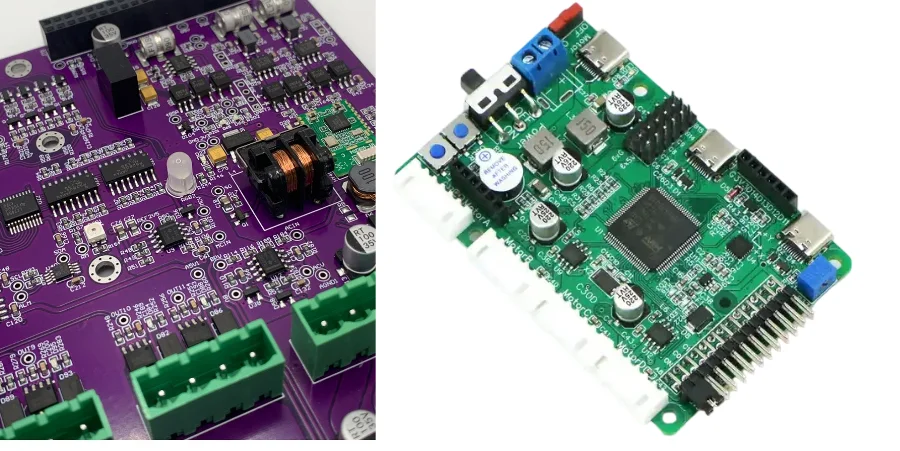
In modern industrial automation, industrial robots serve as the core of smart factories. Their swift and precise movements rely on a "brain" capable of highly efficient computing and a "nervous system" that transmits signals in real-time. Within industrial robot control, PROFINET has become the de facto standard for industrial communication due to its high real-time capabilities, determinism, and extensive bandwidth.
However, integrating PROFINET communication and complex motor control (such as servo drives) onto a single circuit board requires a profound understanding of analog-digital mixed-signal layout, high-voltage/high-current management, and signal integrity. This article explores the best practices in PROFINET control PCB design, detailing how to build a control system that operates reliably in harsh industrial environments, from signal integrity to EMC protection.
PROFINET & Servo Drives: The challenge of mixed-signal coexistence
A typical robot control board usually integrates a microcontroller/FPGA, a PROFINET Ethernet switch/PHY, a servo power stage (inverter), an encoder feedback interface, and various sensor I/Os. PROFINET control PCB design faces the ultimate challenge: how to allow extremely sensitive analog signals (like current sensing), high-speed digital signals (PROFINET), and high-power switching nodes (high dV/dt and di/dt) to coexist harmoniously in a confined space.
The key to solving this lies in strict zoning and layout planning.
Component placement and functional zoning
- Separation of high and low power: The PCB must be physically divided into a high-voltage/high-power zone (inverter circuit, braking resistor, power input) and a low-voltage/control zone (MCU, PROFINET interface, sensors). A sufficiently large isolation gap must be maintained between the two, utilizing optocouplers or digital isolators for signal transmission.
- PROFINET interface isolation: The RJ45 connectors, transformers (magnetics), and PHY chips for PROFINET should be placed as close to the PCB edge as possible. This minimizes Ethernet signal trace lengths and prevents external common-mode noise from contaminating the rest of the board.
- Centralized control: The MCU or FPGA, acting as the system's "brain," should be placed in a "quiet" area within the control zone, keeping the routing of critical signals (like clocks and resets) as short as possible.
Signal Integrity: PROFINET and Encoder Feedback
PROFINET impedance control
PROFINET is based on standard Ethernet physical layers (e.g., 100BASE-TX or 1000BASE-T). Therefore, strict PROFINET control PCB impedance control rules apply.
- Differential impedance: The RX/TX signals between the PHY and the transformer generally require a strict differential impedance of 100 Ω (±10%).
- Avoiding impedance discontinuities: The routing of differential pairs should be as symmetrical as possible, avoiding vias, right-angle turns, and crossing over split reference planes.
- Symmetry: Length differences (skew) within the differential pair must be tightly controlled to prevent timing errors.
Purity of encoder feedback
Servo motors rely on high-resolution encoders (such as BiSS, EnDat, or resolvers) for precise position and velocity feedback. These signals are extremely susceptible to noise originating from the inverter.
- Differential routing: Encoder signals should preferentially be transmitted differentially (e.g., RS-485 levels).
- Decoupling and filtering: Place appropriate RC filters or EMI filters at the encoder interface to attenuate high-frequency noise that might couple from the motor cables.
- Shielding: Ensure a continuous ground plane beneath the encoder signals to provide optimal shielding. A well-designed PROFINET control PCB stackup is the foundation for this.
Best Practices for PROFINET Control PCB Stackup
A well-planned stackup is the foundation for managing EMC and signal integrity. For a typical 6-layer board, the following structure is recommended:
| Layer | Function | Note |
|---|---|---|
| Top | Components, High-speed Signals, Analog Sensors | Keep PROFINET and encoder traces short. |
| Inner 1 | Continuous Ground Plane (GND) | Provides the optimal return path for Top/Inner 2. |
| Inner 2 | General Routing / Internal Signals | For low-frequency or control signal routing. |
| Inner 3 | Power Plane (Power / GND) | Tightly couple with Inner 4 for better decoupling. |
| Inner 4 | Continuous Ground Plane (GND) | Return path for Bottom layer routing. |
| Bottom | Components (optional), High-current Routing | Inverter power traces should be short and wide, using thicker copper. |
Digital Isolation and Common-Mode Rejection: Reliable design for high dV/dt environments
In motor drives, enormous potential differences and severe Common-Mode Transient Immunity (CMTI) events exist between the control side (MCU, FPGA) and the power side (IGBT/MOSFET bridge). Effective electrical isolation is the lifeline for system safety and signal integrity.
- Creepage and Clearance: PCB layout must strictly adhere to relevant safety standards (e.g., IEC 61800-5-1) regarding creepage and clearance distances. This means sufficient physical distance must be maintained on both sides of the isolation boundary, across both surface and inner layers. Creating a keep-out area for all copper layers beneath the isolation boundary is standard practice.
- Digital Isolator Selection: Compared to traditional optocouplers, modern capacitive or magnetic digital isolators offer higher speeds, lower power consumption, longer lifespans, and significantly better CMTI performance. Choosing isolators with high CMTI ratings (>100 kV/μs) is crucial for suppressing the high dV/dt noise generated by motor switching.
- Isolated Power Supply: It is mandatory to provide an independent, isolated power supply for the secondary side (power side) of the isolation barrier. This is typically achieved using isolated DC/DC converters. The layout of the isolated power supply must also follow isolation principles, keeping the PCB area beneath the transformer clear of copper.
- Common-Mode Chokes: Appropriately using common-mode chokes at the PROFINET interface, encoder interface, and power input can effectively filter out common-mode noise, significantly improving the system's immunity.
A successful PROFINET control PCB validation process must include a Hipot Test to verify the integrity and voltage-withstanding capability of the isolation barrier.
Braking Choppers and Energy Absorption: Balancing safety and thermal design
When a robotic arm decelerates or lowers a load, the motor acts as a generator, feeding regenerative energy back into the DC bus, causing the bus voltage to rise. The braking unit (braking chopper) functions to switch an external braking resistor into the circuit when the bus voltage exceeds a threshold, dissipating this excess energy as heat.
Thermal Management
- Braking Resistor Placement: The braking resistor is a major heat source, making its placement on the PCB critical. It should be positioned far away from temperature-sensitive components (like electrolytic capacitors, precision op-amps, MCUs), preferably near the PCB edge or ventilation openings.
- Heat Sinks and Thermal Vias: Large copper polygons should be poured beneath and around the resistor to act as a heat spreader, utilizing dense thermal vias to conduct heat to other layers or a backside-mounted heatsink. This is vital for thermal consistency, from a PROFINET control PCB low volume prototype to PROFINET control PCB mass production.
High-Current Paths and Safety Integration
- Braking Chopper: The power switch (typically an IGBT or MOSFET) controlling the braking resistor, along with its driver circuit, must follow layout rules similar to the main inverter: minimizing power loops to handle the rapid switching of large currents.
- Safety Functions (E-Stop): The braking circuit is usually tightly integrated with the system's safety functions (like Emergency Stop). When a safety stop is triggered, it may be necessary to forcefully activate braking to achieve a rapid, controlled halt. The routing for related relays, drivers, and feedback signals must be reliable and physically isolated from other circuits.
Key Considerations for Braking and Safety Design
- Prioritize thermal management: Keep high-power braking resistors away from sensitive components, utilizing large copper areas and thermal vias for efficient heat dissipation.
- Optimize high-current paths: Traces in the braking chopper circuit should be short and wide to minimize parasitic inductance and resistance, reducing switching losses and voltage spikes.
- Ensure safety circuit integrity: Traces related to the E-Stop and safety relays must be clear, direct, and physically isolated from highly noisy power circuits to guarantee reliable triggering under all conditions.
- Consider component lifespan: Frequent braking operations cause thermal cycling in components. Select high-reliability power devices and resistors with adequate derating during the design phase.
Immunity Design: ESD/EFT/Surge and Return Path Control
Industrial environments are rife with electromagnetic noise such as Electrostatic Discharge (ESD), Electrical Fast Transients (EFT), and Surges. A robust PROFINET control PCB design must possess strong Electromagnetic Compatibility (EMC) performance.
Grounding and Return Path Control
- Unified Ground Plane: For mixed-signal systems containing high-speed digital, sensitive analog, and high-power switching circuits, using a unified, continuous ground plane is best practice. It provides the lowest impedance return path for all signals. Splitting ground planes often causes more problems because return currents are forced to detour, creating large loop antennas that increase EMI radiation and crosstalk.
- Return Path Awareness: When routing, constantly visualize the signal's return path. The return current for high-speed signals tightly follows the path directly beneath the trace on the adjacent reference plane. Routing traces across gaps (splits) in the reference plane is a major taboo in EMC design. An optimized PROFINET control PCB stackup, for example, sandwiching a high-speed signal layer between two ground planes (stripline), provides the best shielding and return path control.
Interface Protection
- TVS Diodes: On the signal lines of all external interfaces (PROFINET, encoder, I/O), TVS (Transient Voltage Suppression) diodes should be placed right next to the connectors to provide a discharge path for transient overvoltages like ESD and EFT.
- Filter Networks: Use π-type or T-type filter networks (composed of capacitors and ferrite beads) to filter out conducted noise entering or leaving the PCB.
Partnering with an experienced manufacturer like HILPCB ensures your design is correctly implemented during manufacturing, whether for rapid iteration in prototype assembly or high-volume production. Their expertise is essential for achieving complex PROFINET control PCB impedance control and sophisticated stack-up structures.
Common Questions
What is the hardest layout problem in PROFINET control PCB design?
The hardest problem is making high-speed communication, sensitive feedback signals, and noisy high-power switching circuits coexist on one board without corrupting each other. That is why strict zoning, short return paths, isolation boundaries, and controlled interface placement are the foundation of the whole design.
Why do isolation and return-path control matter so much in servo and robot controllers?
Because high dV/dt switching and common-mode noise can easily jump into the control side if the isolation boundary and return paths are weak. Good creepage and clearance, strong digital isolators, isolated power, common-mode filtering, and continuous reference planes are what keep the controller safe and the communication stable.
How do teams keep PROFINET and encoder interfaces reliable in harsh industrial environments?
They combine controlled differential routing, short PHY-to-connector paths, clean grounding, local filtering, interface protection, and thermal planning around braking and power stages. Reliability does not come from one EMC part alone; it comes from treating SI, isolation, noise control, and heat as one system.
Conclusion
Successful PROFINET control PCB design is the art of striking the optimal balance between performance, cost, reliability, and safety. It demands that engineers not only understand circuit principles but also possess deep insights into the behavior of high-frequency signals, high-current switching, and sensitive analog signals on the physical PCB. From the layout of the servo drive's power loop to the signal integrity of the encoder interface, to the systematic planning of isolation, thermal management, and EMC strategies, every detail dictates the success or failure of the final product.
Whether you are conducting PROFINET control PCB low volume production for proof-of-concept or heading to market with PROFINET control PCB mass production, adhering to the design principles discussed in this article and partnering with experts like HILPCB, who possess high-speed PCB manufacturing capabilities, will be key to building stable, efficient, and safe industrial robot control systems. Ultimately, an outstanding PROFINET control PCB design empowers your robots with precise motion capabilities and rock-solid reliability.