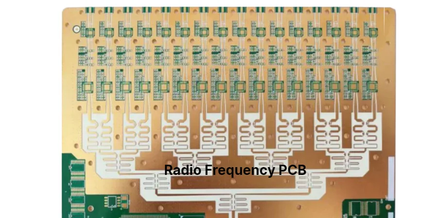
HILPCB specializes in radio frequency (RF) PCB manufacturing and assembly, delivering high-performance boards for wireless communication, radar, satellite, and IoT devices. Our RF PCBs operate from MHz to multi‑GHz ranges, meeting the strict requirements for signal integrity, low loss, and EMI compliance.
We provide complete solutions—from substrate selection to high‑volume manufacturing—helping our customers accelerate time‑to‑market with reliable, production-ready RF PCB designs.
Radio Frequency PCB Design Fundamentals
Radio frequency PCB design requires specialized knowledge of high-frequency signal behavior, transmission line theory, and electromagnetic compatibility principles. RF circuits operating above 100 MHz demand different design approaches compared to conventional digital or analog PCBs due to wavelength effects and signal propagation characteristics.
Essential RF Design Considerations:
• Impedance Control: Precise 50Ω or 75Ω characteristic impedance maintained throughout signal paths with tolerance within ±10% for optimal signal transmission and reflection minimization
• Signal Integrity: Careful trace routing using microstrip, stripline, or coplanar waveguide configurations to control signal propagation and minimize electromagnetic interference
• Layer Stack-up: Optimized layer arrangements with dedicated RF signal layers, ground planes, and power planes ensuring proper isolation and electromagnetic shielding
• Component Placement: Strategic positioning of RF components including amplifiers, filters, and antennas to minimize parasitic effects and maximize circuit performance
Radio frequency PCB designs must account for skin effect losses, dielectric losses, and electromagnetic radiation that become significant at high frequencies. High-frequency PCB substrates with stable dielectric properties ensure consistent performance across operating frequency ranges.
Critical RF Parameters:
Signal wavelength becomes comparable to PCB trace dimensions at RF frequencies, making transmission line effects critical. For 1 GHz signals, traces longer than 425 mils (1/16 wavelength) require controlled impedance design to prevent reflections and signal distortion.
Ground plane continuity becomes essential for RF performance, providing low-impedance return paths and electromagnetic shielding. Any discontinuities in ground planes beneath RF signals can cause impedance variations and performance degradation.
RF PCB Materials and Manufacturing
Professional RF PCB manufacturing relies on advanced materials and precision fabrication to maintain high-frequency performance.
Advanced RF Substrates:
- Rogers RO4003C / RO4350B / RT‑duroid – Low-loss (tan δ≈0.0027), stable dielectric constant
- PTFE Laminates – Ultra‑low loss (tan δ≈0.001) for microwave and radar applications
- Enhanced FR4 – Suitable for lower‑frequency cost‑sensitive RF boards
Precision Manufacturing Techniques:
- Controlled dielectric thickness (±10%) for accurate impedance
- Smooth, low‑profile copper to minimize conductor loss
- Microvias and precision drilling for reduced parasitic inductance
- ENIG or immersion silver finishes for low insertion loss
Comprehensive QC includes TDR, VNA testing, and environmental validation (‑40 °C to +125 °C). Layer registration within ±25 μm ensures differential pair alignment and stable signal integrity.
RF Circuit Types and Design Optimization
RF PCB manufacturing supports multiple circuit types:
- Rigid RF PCBs – Multi‑layer boards with impedance control for transceivers and amplifiers
- Flexible RF PCBs – Polyimide substrates for compact, bendable designs
- High‑Power RF PCBs – Heavy copper PCBs for transmitters >100 W
- Antenna PCBs – PCB traces forming antennas with precise ground plane control
Design & EMI Optimization:
- Keep RF and digital sections ≥20 mm apart; add shielding if <10 mm
- Use 45° or curved traces to reduce reflections and radiation
- Ground stitching vias and guard traces for isolation
- Place decoupling capacitors close to pins to maintain clean power
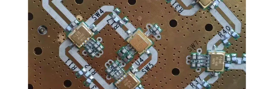
RF PCB Assembly and Testing
High‑precision RF PCB assembly ensures reliable performance for sensitive RF components:
Assembly Capabilities:
- SMT assembly with ±20 μm placement for fine‑pitch RF packages
- Temperature‑controlled reflow profiles to protect sensitive devices
- Grounding and shielding practices to minimize EMI and crosstalk
Testing & Validation:
- S‑parameter and power testing with vector network analyzers
- Spurious emission and regulatory pre‑compliance checks
- Environmental and burn‑in testing for long‑term reliability
RF Applications and Industry Solutions
RF PCB manufacturing supports industries ranging from consumer electronics to aerospace and defense, each requiring precise performance and regulatory compliance. Cellular infrastructure such as base stations and small cells relies on multi‑band RF PCBs with high‑power amplifiers, advanced filtering, and HDI PCB construction for compact layouts. Consumer wireless devices including smartphones, IoT sensors, and smart home products demand space‑efficient RF integration, low‑power operation, and interference mitigation to maintain reliable connectivity.
In industrial, medical, and aerospace applications, RF PCBs face harsher performance and reliability requirements. Radar and satellite systems operating across X‑band to Ka‑band frequencies need specialized substrates, tight phase control, and temperature‑stable designs, while military solutions must meet MIL‑STD environmental standards. Industrial IoT and RFID devices require cost‑effective RF layouts with optimized antennas for long‑range communication, and medical devices demand biocompatible materials and ultra‑low‑power operation for safe and reliable performance.
Professional RF PCB Manufacturing Services
HILPCB delivers end‑to‑end RF PCB solutions from design consultation to mass production:
- RF Design & Simulation – Electromagnetic modeling for first‑pass success
- Material Selection & Guidance – Balance cost and high-frequency performance
- Rapid Prototyping & Testing – Accelerate development with full RF validation
- Scalable Manufacturing – From prototypes to millions of units with consistent quality
Quality & Compliance:
- ISO 9001:2015 and AS9100 certified, ITAR‑compliant for defense projects
- RoHS & REACH documentation for global market access
- Regulatory testing support for FCC, CE, and industry‑specific certifications
Frequently Asked Questions About RF PCBs
Q: What is the typical operating range of an RF PCB?
A: RF PCBs handle signals above 100 MHz, typically from 300 kHz to 300 GHz, requiring controlled impedance and low‑loss materials.
Q: Which materials are best for RF PCBs?
A: Rogers RO4003C/4350B and PTFE laminates offer excellent high‑frequency performance, while enhanced FR4 is suitable for lower‑frequency RF boards.
Q: How is impedance control achieved?
A: By precise trace geometry, dielectric control, and stackup design, verified with TDR to maintain ±5% tolerance.
Q: What are the critical assembly considerations?
A: Precise placement, shielding, proper grounding, and temperature‑controlled reflow to protect sensitive RF components.
Q: Can HILPCB support high‑power RF applications?
A: Yes, we provide solutions from low‑power IoT to >100 W transmitters, including heavy copper designs and specialized RF assembly.