As data centers advance toward 800G and even 1.6T speeds, the power consumption and thermal density of pluggable optical modules such as QSFP-DD and OSFP have reached unprecedented levels. Integrating high-speed DSP chips, laser drivers, TIAs, and passive components into a high-performance PCB within such a compact space presents extreme challenges for SMT assembly processes. This is not merely about component placement but involves a systems engineering approach that couples optical, electrical, thermal, and mechanical considerations. A successful SMT assembly solution must integrate thermal management, signal integrity, and long-term reliability from the very beginning of the design phase.
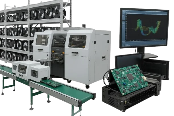
At HILPCB, we understand the complexity of optical module manufacturing, which demands SMT production lines not only capable of high-precision placement but also proficient in hybrid assembly processes like THT/through-hole soldering to meet the installation requirements of connectors and cages. This article will delve into the core challenges and solutions of SMT assembly for data center optical module PCBs from the perspective of connector and fiber engineers.
TEC and Thermal Path Synergy: Heat Flow Management from Chip to Heat Sink
The primary heat sources in optical modules—DSP chips and lasers—are highly sensitive to operating temperatures. Particularly for lasers, wavelength stability directly depends on precise temperature control, typically achieved by thermoelectric coolers (TECs). Efficient thermal management begins with an unobstructed thermal path from the chip to the external heat sink (cage).
This path spans the entire PCB structure: heat generated by the chip is conducted through TIM (thermal interface material) to the copper foil and thermal pads on the PCB, then rapidly transferred to the backside of the PCB via dense arrays of thermal vias, and finally dissipated through contact with the module housing or heat sink. During SMT assembly, ensuring a low thermal resistance connection between BGA-packaged DSP chips and the PCB is critical. This is where Low-void BGA reflow technology plays a pivotal role. Through vacuum reflow soldering or optimized temperature profiles, we minimize voiding under BGA solder joints, maximizing thermal conduction efficiency and preventing localized chip overheating. A well-designed high-thermal-conductivity PCB is the foundation for achieving this goal.
CTE Matching and Low Warpage: The Cornerstone of High-Density Interconnect Reliability
Optical module PCBs integrate components with diverse material systems: silicon-based DSP chips, ceramic-based TOSA/ROSA, and organic resin-based PCBs. These materials exhibit significant differences in coefficient of thermal expansion (CTE). During the extreme temperature fluctuations of reflow soldering (from room temperature to over 250°C) and the thermal cycling of long-term operation, CTE mismatch generates substantial mechanical stress, directly threatening the reliability of BGA and other precision solder joints.
To address this challenge, our strategy includes:
- Material Selection: Use low-CTE high-speed PCB materials like Megtron 6 or Tachyon 100G to minimize expansion mismatch with chips.
- Stackup Design: Adopt symmetrical stackup structures to balance internal stress and effectively suppress PCB warpage during SMT assembly.
- Process Control: Precise Low-void BGA reflow processes not only enhance thermal performance but also create more robust solder joints resistant to stress fatigue. For high-reliability applications, Conformal coating may also be considered to further reinforce solder joints against environmental stress.
Core Challenges in Optical Module Assembly
- Thermal Management: Power consumption exceeding 20W concentrated within a few square centimeters requires a thermal resistance path from chip to heat sink of less than 1-2°C/W.
- Mechanical Stress: Significant CTE differences between chips, ceramics, and PCBs can easily lead to BGA solder joint failure under temperature cycling.
- Signal Integrity: 112Gbps PAM4 signals are extremely sensitive to impedance, crosstalk, and jitter. Any assembly flaws may cause link failure.
Reflow Profile and MSL (Example)
| Stage/Parameter | Typical Range/Practice | Key Points |
|---|---|---|
| Preheat/Soak | 0.5–3°C/s;150–200°C,60–120 s | Activation and Soaking, Anti-Solder Splashing |
| Peak/Liquidus Time | 235–250°C; TAL 30–90 s | Combined with Vacuum/Nitrogen to Reduce BGA Voids |
| MSL Control | Follow Datasheet Exposure Limits and Baking | MES-Binded Reflow/Baking Records |
Note: This is a generic example; refer to solder paste/device/substrate data and solidify in FAI to SOP/MES.
Cleaning and Optical Assembly Synergy
- Select compatible flux/cleaning systems to reduce ionic residues; perform ROSE/SIR sampling after cleaning
- Control volatilization and curing curves before optical assembly to avoid impact on coupling and adhesive materials
- Selective coating for critical areas; avoid contamination of optical surfaces and connector contacts
Testing and Traceability
- Establish SPI/AOI/X-Ray data closed-loop with SPC/MES; anomalies trigger line stoppage/retesting
- Bind I2C/CMIS firmware versions and checksums to serial numbers; record JTAG structural test coverage for interconnects
Power Allocation and Signal Integrity for PAM4 High-Speed Links
While PAM4 modulation technology increases data rates, it also imposes higher demands on DSP equalization algorithms, leading to a sharp rise in power consumption. Providing stable, clean power to these "power-hungry" chips is a prerequisite for ensuring signal quality (e.g., eye diagram opening and low jitter). This requires the power distribution network (PDN) to exhibit extremely low impedance.
During the SMT assembly phase, this means placing a large number of decoupling capacitors as close as possible to the DSP's power pins. High-density layouts pose challenges for automated optical inspection (AOI), and for BGA solder joints that cannot be directly probed, Boundary-Scan/JTAG testing becomes a critical method to verify soldering quality and electrical connectivity. Through the JTAG interface, we can check the connection status of each pin without physical probes, ensuring PDN integrity. Additionally, a well-designed Fixture design (ICT/FCT) solution is indispensable for validating PAM4 link performance, as it ensures stable power delivery and high-speed signal acquisition during subsequent testing.
Advanced Testing and Validation: Ensuring Assembly Quality and Long-Term Reliability
The "zero-defect" requirement for optical modules means testing must be integrated throughout the process. At HILPCB, our SMT Assembly process incorporates multi-level testing strategies to ensure every delivered PCBA meets the most stringent standards.
- Online Testing (ICT/FCT): We develop customized test fixtures for each optical module. Precise Fixture design (ICT/FCT) ensures accurate contact with tiny test points, enabling power supply, low-speed signal communication, and basic functional verification.
- JTAG Testing: For complex components like BGAs and FPGAs, Boundary-Scan/JTAG is the preferred solution to verify the integrity of all pin soldering. It detects open or short-circuit defects that traditional optical or electrical tests cannot identify.
- Environmental and Reliability Testing: Finished modules undergo rigorous temperature cycling and aging tests to screen for early failures. In scenarios requiring resistance to harsh environments (e.g., edge computing nodes), we also apply Conformal coating to provide moisture, dust, and corrosion protection for PCBA.
HILPCB Assembly Advantages
- ✓ Advanced Process Capabilities: Mastery of vacuum reflow soldering technology achieves Low-void BGA reflow, ensuring exceptional thermal performance and reliability.
- ✓ Comprehensive Test Coverage: Combines AOI/AXI, Boundary-Scan/JTAG, and customized Fixture design (ICT/FCT) to ensure a 100% defect detection rate.
- ✓ Hybrid Technology Expertise: Seamlessly integrates SMT assembly with THT/through-hole soldering, offering one-stop services from PCB manufacturing to complete module assembly.
- ✓ Reliability Assurance: Provides value-added services like Conformal coating to enhance product lifespan in harsh environments.
Hybrid Assembly Process: Synergistic Application of THT and SMT
Although optical modules primarily use SMT components internally, their external interfaces—such as board-edge connectors and metal cages—often employ through-hole technology for stronger mechanical retention. This requires the assembly process to efficiently integrate both SMT and THT/through-hole soldering techniques. In a typical process, we first complete double-sided SMT placement and reflow soldering, then use selective wave soldering or manual soldering to install through-hole components. This process requires precise masking and temperature control to protect adjacent SMT components from secondary high-temperature exposure. The entire Turnkey Assembly process design, including the setup of THT/through-hole soldering stations, is meticulously optimized to ensure maximum efficiency and consistent soldering quality. Finally, all assembled PCBAs undergo final functional testing and cleaning, followed by Conformal coating treatment as per customer requirements, preparing them for final module enclosure installation.
Conclusion
SMT assembly for data center optical modules is a highly complex systems engineering task that extends far beyond traditional PCBA assembly. It requires manufacturers to have deep expertise in high-speed signals, thermodynamics, and advanced manufacturing processes. Every step is critical—from achieving Low-void BGA reflow to optimize thermal pathways, to leveraging Boundary-Scan/JTAG for electrical connectivity verification, and integrating THT/through-hole soldering to enhance mechanical strength.
With years of experience in high-speed PCB manufacturing and complex electronic assembly, HILPCB provides customers with a one-stop solution spanning design optimization, PCB fabrication, and final module assembly. We are committed to helping clients overcome optoelectronic co-design and thermal challenges through advanced SMT assembly technologies, accelerating the time-to-market for next-generation data center products.