
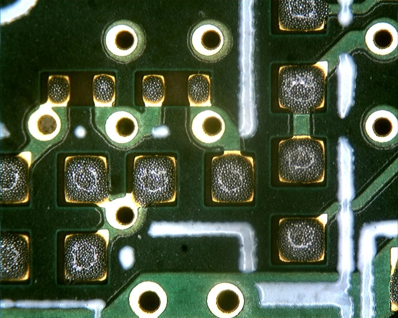
Solder paste inspection (SPI) checks the paste printed on a PCB before components are placed. A useful SPI result identifies the deposit, compares its measured geometry with an approved recipe, and tells the operator whether to release the board or investigate the print. A passing result does not establish the quality of the solder joints that will form later.
For a new assembly, agree on the inspection coverage, pad-family limits and failed-print disposition before production. SMT stencil design determines the intended deposit; SPI checks what the printer delivered. Automated optical inspection addresses placement and visible assembly features at later stages.
What does an SPI machine measure?
SPI in SMT means inspection of solder paste, rather than the Serial Peripheral Interface used for communication between chips. The SPI machine normally sits between the stencil printer and component placement. It can catch a printing problem while the affected board is still available for an approved cleaning and reprint procedure.
A 3D solder paste inspection system reconstructs the deposit surface and derives its height and volume. Area, position and shape complete the picture. For example, GÖPEL's Vario Line specification lists height, area, volume, offset, shape, bridges and coplanarity as inspection criteria. The available measurements depend on the equipment and programmed inspection region. GÖPEL measurement criteria.
| Result | Question it answers | What else must be checked |
|---|---|---|
| Volume | How much paste is inside the measured region? | The nominal reference, aperture revision and whether a bridge extends outside that region |
| Height | How high is the deposit above the taught surface? | Board support, local reference plane and the shape of the deposit |
| Area | How much of the programmed footprint contains paste? | A wide, shallow deposit may cover enough area but contain too little volume |
| X/Y offset | How far has the deposit moved from its intended position? | Alignment across the panel, fiducial teaching and the actual pad geometry |
| Shape and bridging | Is the paste contained in the intended pattern? | Separate deposits must not be accepted merely because their combined volume looks correct |
How does 2D differ from 3D solder paste inspection?
A 2D image can compare paste coverage and position but does not directly measure deposit height. 3D solder paste inspection adds height information for volume measurement. This matters when small deposits have similar top views but different amounts of paste.
Some equipment uses projected fringe patterns and optical reconstruction. Multiple projection directions can reduce shadowing, while reference-plane and warpage compensation address errors caused by the board surface. These are equipment features to verify, rather than reasons to assume every measurement is exact. Koh Young's technology description explains those effects for its own systems.
When comparing an SMT SPI machine for a fine-pitch build, ask for repeatability evidence on the relevant deposit sizes and surface finish. A nominal camera resolution alone does not demonstrate that the inspection can distinguish an acceptable print from the smallest rejectable one.
Why can a thicker stencil produce a less consistent print?
A thicker stencil increases the geometric aperture volume, but it also increases the wall area from which the paste must release. Both effects matter when choosing the print process.
For a straight-sided rectangular aperture, area ratio is opening area divided by aperture-wall area:
Area ratio = W × L / [2 × (W + L) × T]
Here, W and L are aperture dimensions and T is foil thickness. A square aperture simplifies to W / (4 × T); a circular aperture of diameter D has area ratio D / (4 × T). Indium describes roughly 0.66 as a conventional release guideline: below it, transfer can become low or variable, although improvements in paste technology can change that behavior. It is not a universal SPI acceptance threshold. Indium, Minimizing Graping.
The following calculated example keeps a square aperture at 0.30 × 0.30 mm and changes only foil thickness. It assumes straight walls and is not a measured production result.
| Foil thickness | Theoretical aperture volume: W × L × T | Area ratio | Decision before release |
|---|---|---|---|
| 0.100 mm (100 µm) | 0.00900 mm³ | 0.75 | Check whether the deposited volume satisfies the joint requirement |
| 0.125 mm (125 µm) | 0.01125 mm³ | 0.60 | Verify actual release and variation; the larger hole volume does not ensure more usable paste |
The thicker foil has 25% more theoretical volume. Transfer efficiency is measured deposit volume divided by aperture volume, so a reduction in transfer can offset that increase. Compare the SPI distributions and post-reflow results before selecting the foil. Aperture changes, paste selection or a step stencil may resolve a mixed-package conflict; reducing thickness everywhere can leave larger joints short of solder.
How should SPI limits be set for a new assembly?
Define what “100% volume” means in the inspection recipe. It may refer to aperture area multiplied by foil thickness, but an agreed target or taught reference must be identified explicitly. Two suppliers' percentage reports are not comparable if their denominators differ.
Group deposits by function: small BGA lands, QFN perimeter pads, segmented thermal pads, chip components and large connector pads may require different targets and response limits. For a windowpane thermal-pad pattern, record whether the recipe evaluates individual deposits, the combined pattern, or both.
The NPI release sequence should establish:
- The input revision. Match the paste data, approved stencil drawing, board revision and component package information to the SPI program.
- Measurement suitability. Check registration, local height reference and repeatability before interpreting a marginal result as a printer fault.
- The process window. Evaluate repeat prints and correlate critical deposits with placement and post-reflow findings. Approve limits with the responsible process and quality engineers.
- The response rule. Distinguish a warning trend from a rejected print, identify who can authorize a disposition, and retain the original result after any adjustment.
IPC-7527 addresses solder paste printing, while IPC-A-610 concerns assembly acceptance. The public IPC-7527 scope also recognizes the need for unique acceptance criteria in some applications. Specify the contractual revisions and customer requirements; a workmanship class alone does not supply a complete SPI recipe.
What should happen when SPI inspection flags a print?
Use the location and pattern of an alarm to choose the next check. A single low-volume result is not enough to identify a unique cause.
| Observed pattern | Check the measurement first | Investigate at the printer | Evidence to retain before release |
|---|---|---|---|
| Low volume repeats on the same small apertures | Correct aperture reference and inspection region | Blockage, paste condition and release geometry | Deposit trend before and after the correction, linked to stencil revision |
| Similar offset across the panel | Fiducial teaching and board registration | Alignment and tooling movement | Alignment correction and repeat inspection result |
| Height varies by board region | Local reference plane and warpage compensation | Support arrangement, board flatness and stencil contact | Regional measurements after support or setup changes |
| Paste connects adjacent deposits | Image and bridge detection region | Underside contamination, print alignment and paste behavior | Recorded disposition and confirmation that the repeated print is separated |
| One chip component has unequal deposits | Pad pairing and target definitions | Local release or aperture imbalance | Paired deposit results plus relevant post-reflow observations |
Hold a rejected board before placement. Cleaning and reprinting require an approved method compatible with the board, finish, paste and any components already present on the opposite side. Define residue removal, drying, inspection and permitted repeat processing in that procedure. A wipe is not automatic permission to send the board back into production.
Closed-loop printer feedback can correct selected trends where the equipment integration supports it. Confirm which parameters can change automatically, how changes are logged, and when the operator must intervene. Do not widen a limit just to remove an alarm without evaluating the effect on the joint.
What does SPI leave for AOI, X-ray and electrical test?
SPI solder paste inspection controls the printed material before placement. It cannot show whether that material later wets the terminals, whether a BGA joint connects electrically, or whether the product functions.
Post-reflow AOI checks accessible assembly features. X-ray PCB inspection addresses selected hidden-joint questions, including solder distribution under packages; its coverage depends on the method and viewing geometry. Electrical and functional testing require their own test points, programs and acceptance limits. Plan these together in the SMT assembly process.
When judging the cost of SPI, compare programming and inspection effort with the actual cost of containment, cleaning, reprinting and later rework on your assembly. Ask suppliers to distinguish stencil changes and NPI setup from recurring inspection and record-delivery charges. A generic percentage improvement in yield does not establish savings for a different board.
What should the RFQ and first-build release package contain?
Send versioned paste and solder-mask layers, assembly drawings, the bill of materials, placement coordinates and component package notes. Identify critical BGA/QFN locations, small passive pairs, thermal-pad patterns and any customer-controlled stencil design. State the board quantity, assembly sides, workmanship requirements and required traceability.
Before signing off the build, request:
- A coverage statement defining inspected sides, deposits, sampling or full inspection, and any exclusions.
- The approved SPI recipe revision, pad groups, nominal references and warning/reject limits.
- Critical-deposit results linked to the relevant panel or lot, with the agreed output format and retention period.
- The hold, cleaning, reprint and concession process, including who releases a previously rejected board.
- NPI evidence connecting print findings with the specified post-reflow inspection and test results.
The assembler owns process setup and execution. The buyer and designated quality authority approve the contractual evidence and any concessions. Product-level qualification remains a separate responsibility; an SPI report cannot release the whole system.
HILPCB's SMT assembly capability includes 3D SPI and 2D/3D AOI, with selected X-ray for agreed hidden-joint risks. The inspection route, coverage and requested records are confirmed at quotation. Submit the assembly package and inspection requirements when you request a quote.
FAQ
What is solder paste inspection used for?
It checks printed solder paste before component placement. Height, volume, area, position and shape measurements help identify print errors and process drift while the board can still be held for correction.
Is solder paste testing the same as SPI?
Solder paste testing can refer to incoming material tests or print-process checks. SPI measures the deposited paste on a board; it does not replace the paste supplier's material specification or the assembly's post-reflow tests.
What should a solder paste inspection wiki definition include?
It should identify the inspection timing, measured deposit geometry and limits of the result. A definition should also distinguish solder paste inspection from the Serial Peripheral Interface, which shares the abbreviation SPI.
Does an SPI 3D result prove that a BGA joint is good?
No. It measures the paste before the BGA is placed and reflowed. Hidden-joint inspection and electrical testing must address the later assembly risks specified in the quality plan.
Can one solder paste inspection system use the same limits for every board?
A system can store multiple recipes, but each board's limits need an approved reference and validation. Different apertures, foil thicknesses, packages and paste materials can require different targets and limits.
Can a board that fails SPI be cleaned and reprinted?
Potentially, under an approved disposition. The cleaning method, drying, inspection and permitted repeat processing must suit the board and materials, including any components already fitted. Retain the failed result and the subsequent release evidence.