
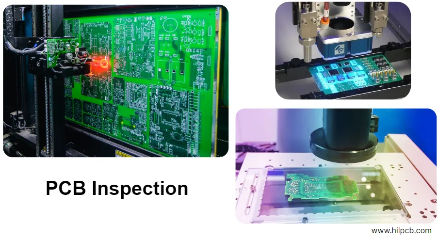
In modern printed circuit board manufacturing and surface-mount technology (SMT) assembly, AOI (Automated Optical Inspection) is the indispensable automated machine-vision quality gate that inspects circuit boards for visual and physical defects. Understanding what is AOI, the fundamental AOI meaning, and how automated optical inspection systems operate is critical for hardware designers, production engineers, and quality assurance managers.
As microelectronics miniaturize toward 01005 (0402 metric) passives and ultra-fine-pitch 0.35 mm BGAs, human visual inspection through microscopes is neither statistically repeatable nor commercially viable. An inline AOI inspection system scans thousands of solder joints per minute with micrometer accuracy, capturing solder defects, component misalignments, and polarity errors before boards advance to end-of-line functional testing.
What Does "AOI" Stand For? (AOI Meaning)
AOI stands for Automated Optical Inspection (or alternately Automatic Optical Inspection).
An AOI machine is an autonomous, computer-controlled vision platform that captures high-resolution digital images of printed circuit boards under calibrated multi-angle lighting. Advanced computer-vision algorithms, statistical image comparisons, or artificial intelligence (AI) neural networks compare each inspected board against a computerized golden reference model or CAD design files.
The Inspection Trinity: SPI vs. AOI vs. AXI
In a tier-1 SMT assembly line, optical inspection is deployed across multiple sequential checkpoints:
+---------------------------------------------------------------------------------+
|                              SMT Process Inspection Gates                       |
+---------------------------------------------------------------------------------+
| 1. Solder Paste Stencil Printing ---> [ 3D SPI (Solder Paste Inspection) ]      |
| 2. High-Speed Pick-and-Place     ---> [ Pre-Reflow AOI (Optional Component Check) ] |
| 3. Convection Reflow Soldering   ---> [ Post-Reflow 3D AOI (Solder Joint Quality) ] |
| 4. BGA / QFN Concealed Joints    ---> [ 3D AXI (Automated X-Ray Inspection) ]  |
+---------------------------------------------------------------------------------+
- SPI (Solder Paste Inspection): Positioned directly after the solder stencil printer. It measures solder paste deposit volume, height, area, and registration before components are placed. Over 65% of SMT soldering defects originate at the printing stage.
- Pre-Reflow AOI: Positioned after component placement but before the reflow oven. It catches missing parts, polarity errors, and lateral skew before solder melts, allowing simple rework without thermal stress.
- Post-Reflow AOI: Positioned immediately after the reflow oven. It inspects completed solder joints for wetting, bridges, lifted leads, tombstoning, and solder volume.
- AXI (Automated X-Ray Inspection): Complements optical inspection by using penetrating X-rays to inspect hidden joints (e.g., solder balls beneath BGAs, LGA pads, and QFN ground pads) where optical line of sight is obstructed.
How AOI Works: Optics, Lighting, and Machine Vision
An industrial AOI inspection machine combines precision linear motor gantries, telecentric optical lenses, multi-wavelength LED illumination arrays, and high-performance digital image processing.
1. Optical Imaging System
High-resolution CMOS cameras (ranging from 5 to 25 megapixels) capture digital frames of the PCB surface. Telecentric lenses are employed to eliminate optical perspective distortion—ensuring that components at the edge of the field of view (FOV) are measured with the exact same dimensional accuracy as components in the optical center.
2. Multi-Tier RGB Lighting
Solder joints act as microscopic mirrors. When molten solder wets a copper pad and component termination, it forms a curved concave meniscus. AOI systems exploit this curvature using multi-angle, multi-color LED rings (typically red, green, and blue LEDs positioned at varying elevation angles):
- High-angle (top) lighting reflects off flat horizontal surfaces (e.g., component tops, pad surfaces).
- Mid-angle lighting highlights moderately sloped solder fillet transitions.
- Low-angle grazing lighting reflects off steep fillet edges and solder bridging between pins.
By analyzing the resulting color distribution in the camera image, the vision algorithm instantly reconstructs the shape and slope of every solder fillet.
3. Image Analysis Algorithms
Modern AOI software analyzes captured imagery through three complementary processing methodologies:
- CAD-to-Image / Template Matching: Compares the inspected board against a verified golden board image, flagging pixel differences beyond programmed tolerance bands.
- Statistical Color Profiling (SCP): Calculates statistical color and brightness values across hundreds of verified good solder joints to create dynamic pass/fail envelopes.
- AI & Deep Learning Classification: Neural networks trained on millions of real-world SMT defects distinguish genuine solder defects from harmless cosmetic variations (such as solder mask color shifts or silk-screen bleed), reducing operator verification fatigue and false call rates.
2D AOI vs. 3D AOI: Technology Comparison
The transition from traditional 2D optical inspection to modern 3D AOI represents the single biggest technological leap in SMT quality engineering.
Limitations of Traditional 2D AOI
2D AOI systems evaluate circuit boards purely from flat, planar optical images ($X$ and $Y$ dimensions). While effective for detecting missing components or gross solder bridges, 2D AOI cannot measure true physical height ($Z$ dimension). As a result, 2D AOI struggles with:
- Lifted leads and component coplanarity defects (a lead raised 50 µm above a pad often looks identical in 2D top-down view).
- High false call rates (FCR): Variations in solder paste reflectivity, component silk-screen markings, or board PCB warpage cause 2D systems to trigger thousands of false alarms, overwhelming review stations.
Advantages of 3D AOI (Phase-Shift Profilometry)
3D AOI projects structured moiré fringe patterns onto the circuit board using digital light projectors. By measuring the phase shift and distortion of the fringe patterns from multiple triangulation cameras, the system calculates the absolute height ($Z$) of every pixel with 1 µm resolution.
3D AOI provides true volumetric measurement of solder joints, precise component tilt angles, and coplanarity verification, completely immune to shadow effects, component color changes, or PCB surface warpage.
| Capability / Metric | Traditional 2D AOI | Modern 3D AOI Systems |
|---|---|---|
| Measurement Dimensions | $X, Y$ planar coordinates only | True $X, Y, Z$ volumetric coordinate profiling |
| Height Measurement | None (inferred indirectly from color reflection) | Direct physical height measurement ($\pm 1 \ \mu\text{m}$ resolution) |
| Lifted Lead Detection | Low reliability (reflection sensitive) | 100% reliable height coplanarity verification |
| Solder Volume Measurement | 2D area estimate only | Quantitative volumetric measurement ($µ\text{m}^3$) |
| Component Tilt & Tombstone | Difficult on miniature chips (0201 / 01005) | Precise angular tilt ($\theta$) measurement |
| Board Warpage Compensation | Causes focal blur and measurement errors | Real-time dynamic $Z$-plane mapping and compensation |
| False Call Rate (FCR) | Typically 1,000 – 3,000 ppm | Dramatically reduced (< 200 – 400 ppm) |
| Inspection Speed | Extremely fast (single top exposure) | Fast (high-speed structured light projection) |
Defect Detection Capabilities: What AOI Catches vs. What It Misses
For quality managers and procurement teams, knowing the exact capability boundary of an AOI machine is vital for designing an airtight test strategy.
Defects AOI Reliably Catches
- Missing Components: Complete absence of passive chips, transistors, or IC packages.
- Component Skew and Misalignment: Angular rotation, lateral $X/Y$ offset, or overhang exceeding IPC-A-610 limits.
- Tombstoning (Manhattan Effect) & Billboarding: Components standing vertically or resting on their side edge.
- Polarity and Pin 1 Orientation: Incorrect orientation of electrolytic capacitors, diodes, LEDs, and ICs verified by optical polarity markings or laser-etched notches.
- Wrong Part Placement: Optical Character Recognition (OCR/OCV) reads alphanumeric markings on IC tops to ensure correct bill-of-materials (BOM) values.
- Solder Bridging (Shorts): Unintended copper or solder shorts spanning between fine-pitch IC pins.
- Insufficient Solder / Dry Joints: Thin solder fillets, lack of wetting, or de-wetting on pads.
- Excess Solder / Solder Balls: Spattered solder balls or oversized solder joints violating electrical spacing.
Defects AOI Cannot Detect (Inherent Limitations)
- Hidden Solder Joints (BGA, QFN, LGA): AOI relies on optical line of sight. Solder balls directly underneath Ball Grid Arrays (BGAs) or ground thermal pads beneath QFN packages cannot be inspected with optical cameras. Solution: Requires 3D Automated X-Ray Inspection (AXI).
- Internal Solder Joint Voids: IPC-A-610 Class 3 mandates that voiding within BGA solder spheres must not exceed 25% of total ball area. Optical systems cannot penetrate solder mass to measure internal gas voids. Solution: 3D X-Ray inspection.
- Internal PCB Laminate Defects: Inner-layer trace opens, delamination, dielectric blistering, or barrel plating cracks inside vias are invisible to surface AOI. Solution: In-circuit testing (ICT), flying probe electrical testing, and cross-section microsectioning.
Frequently Asked Questions (FAQ)
What is AOI in electronics manufacturing?
In electronics manufacturing, AOI (Automated Optical Inspection) is an automated machine-vision testing method used on SMT production lines to visually inspect printed circuit boards and electronic assemblies for solder joint defects, component placement errors, and polarity faults.
What does AOI stand for?
AOI stands for Automated Optical Inspection (or Automatic Optical Inspection).
Can AOI inspect BGA and QFN components?
AOI can only inspect the outer visible perimeter leads of QFNs or verify that a BGA package is present, aligned, and seated at the proper height. It cannot inspect the concealed solder balls underneath the BGA or the ground pad beneath the QFN, which require Automated X-Ray Inspection (AXI).
What is the primary difference between 2D and 3D AOI?
2D AOI captures flat planar ($X, Y$) photographs and evaluates defects through color and brightness contrast, which frequently leads to false alarms caused by lighting reflections. 3D AOI uses structured fringe projection to measure true physical height ($Z$) and volume, reliably detecting lifted leads, component tilt, and solder volume.
HILPCB Advanced 3D AOI and Quality Inspection Services
At HILPCB, every bare board and turnkey circuit board assembly passes through a multi-tiered inspection pipeline built on industry-leading equipment:
- 100% Inline 3D SPI and 3D AOI: High-precision Koh Young 3D optical inspection platforms detect solder volume deviations and placement skew with micron-level accuracy.
- Comprehensive 3D X-Ray (AXI) Capabilities: Automated non-destructive X-ray imaging for 100% inspection of concealed BGA, LGA, and QFN solder joints.
- IPC-A-610 Class 2 & Class 3 Compliance: Calibrated inspection recipes adhere to strict IPC acceptance criteria, backed by certified inspectors.
- Full Electrical Verification: In-circuit testing (ICT), flying probe testing, and custom functional testing (FCT) guarantee complete electrical integrity.
Upload your Gerber and BOM files to HILPCB today to get a comprehensive DFM/DFA review and instant manufacturing quotation.