
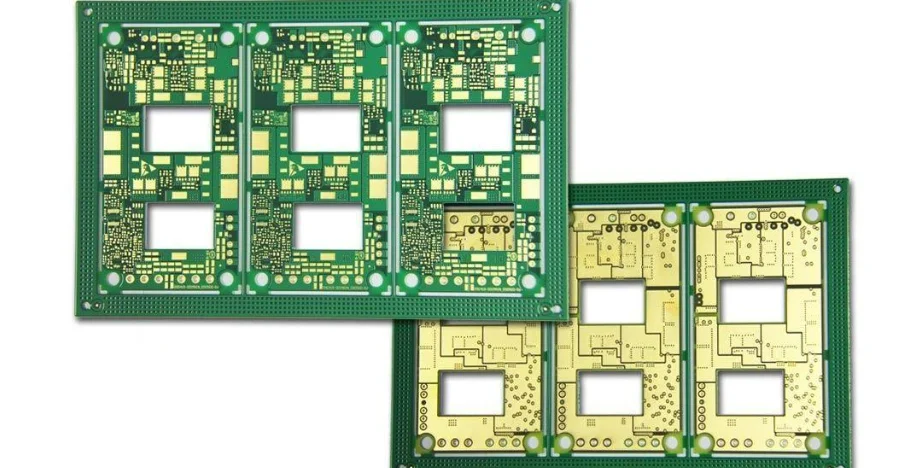
In medical imaging and wearable devices, reliability and safety are not only the core of competitiveness—they are non-negotiable regulatory red lines. As a reliability and compliance engineer working with IEC 60601 and ISO 10993, I’ve seen how small defects in design or manufacturing can lead to severe consequences. A comprehensive SPI/AOI/X-Ray inspection flow is therefore foundational to ensuring medical-grade PCBs meet the highest standards from design validation through mass production. This “combo” inspection stack runs through the entire lifecycle, safeguarding electrical safety, biocompatibility, and long-term stability.
Medical products—especially those that directly or indirectly contact the human body—have a development process far more complex than consumer electronics. Starting at NPI EVT/DVT/PVT, regulatory requirements must be embedded into every detail of design and manufacturing. SPI/AOI/X-Ray inspection is no longer just a solder-defect finder; it becomes a hub for validating design rules, monitoring process stability, and generating traceable compliance evidence. At HILPCB, we use these capabilities to provide end-to-end compliance assurance from prototype to volume production.
IEC 60601 key clauses: how SPI/AOI/X-Ray inspection protects electrical safety
IEC 60601 is widely regarded as the “bible” for medical electrical equipment safety and essential performance. Requirements for leakage current, clearance, and creepage are strict and directly tied to patient/operator safety. Potential interconnect failures—solder bridging, component offset, or micro-defects under insulation—can cause excessive leakage or insulation breakdown.
SPI/AOI/X-Ray inspection plays a preventive and in-process monitoring role:
- Solder paste inspection (SPI): As the first gate in SMT assembly, SPI measures paste volume/area/height. Inaccurate printing is a root cause for a large portion of solder defects. Controlling paste prevents bridging (reducing creepage) and insufficient solder (weak joints impacting long-term electrical reliability).
- Automated optical inspection (AOI): After placement and reflow, AOI compares high-resolution PCB images to golden standards to detect offset, polarity errors, wrong/missing parts, and obvious solder defects. For parts where clearance/creepage is critical, accurate placement is a key AOI focus.
- X-Ray inspection: For bottom-terminated packages such as BGA and QFN, optical inspection cannot see the joints. X-Ray reveals internal solder-joint geometry and finds critical defects like bridging, Head-in-Pillow, Voids, and cracks—major electrical-safety risks under IEC 60601.
Throughout NPI EVT/DVT/PVT, inspection data feeds design and process optimization (pad design, solder mask openings, reflow profiles), ensuring compliance before mass production. For high-insulation needs such as high Tg PCB, X-Ray helps confirm solder quality under complex packages to maintain strong electrical performance.
ISO 10993 biocompatibility: end-to-end control from materials to Potting/encapsulation
For wearables, implantables, or any device with long-term body contact, ISO 10993 biocompatibility is mandatory. All materials that may contact the body must not cause toxicity, irritation, or sensitization—including enclosure materials, PCB laminates, solder mask inks, components, and protective coatings.
Potting/encapsulation is one of the key processes to achieve biocompatibility. Using medical-grade silicone or epoxy, the entire PCBA can be fully encapsulated to form an inert, dense barrier isolating internal electronics from the human environment. But the protection effectiveness depends on process quality.
SPI/AOI/X-Ray inspection extends into protection verification:
- Upstream SMT assembly quality assurance: A reliable Potting/encapsulation starts with a clean, defect-free PCBA. AOI helps ensure no residues or latent corrosion sources exist before encapsulation and that solder joints are secure.
- Post-potting validation: X-Ray is the ultimate method to evaluate potting quality. It can see through opaque materials to check for bubbles, voids, or delamination. Such defects reduce protection against moisture/body fluids and may create stress concentrators that crack over time, potentially exposing non-biocompatible materials.
By combining SPI/AOI/X-Ray inspection with strict material control, we ensure every step from PCB material selection to final Potting/encapsulation meets ISO 10993 expectations, providing hard evidence for biosafety.
Comparison of inspection and test technologies for medical devices
| Technology | What it inspects | Key advantage | Role in medical compliance |
|---|---|---|---|
| SPI (solder paste inspection) | Solder paste before reflow | Prevents defects at the source; quantifies process control | Prevents shorts/opens from too much/too little paste; supports electrical safety |
| AOI (automated optical inspection) | Visible components and joints | Fast, efficient, broad coverage | Ensures placement/polarity correctness; supports clearance requirements |
| X-Ray inspection | Hidden joints (BGA, QFN) and internal structures | Only method to see hidden defects | Finds BGA bridging/weak joints; verifies Potting/encapsulation integrity |
| Flying probe test | Electrical connectivity of nets | No fixture required; flexible; ideal for prototypes | Fast circuit verification in NPI; finds design/early-process issues |
Reliability qualification: SPI/AOI/X-Ray inspection in environmental stress screening
Medical devices must remain stable across their intended lifetime—whether in complex hospital EMI environments or under day-to-day temperature/humidity change and mechanical shocks. Thermal cycling, damp heat, vibration, drop, and sweat corrosion testing are common forms of ESS.
SPI/AOI/X-Ray inspection becomes a “defect magnifier” in this phase. Latent defects that do not appear at room conditions can be exposed under stress:
- Pre-test baseline: Before stress tests, perform X-Ray on the PCBA—especially BGA—to establish a baseline “healthy” joint image archive.
- Post-test comparison: After thousands of thermal cycles or long vibration runs, X-Ray the same locations again. Comparing before/after images reveals Micro-cracks driven by CTE and mechanical stress—often not an immediate functional failure, but a time bomb for future field issues.
This “test–inspect–analyze” closed loop is central to reliability growth. It validates the durability of materials such as flex PCB in dynamic use and also validates process robustness of SMT assembly. When defining test strategies, strong Fixture design (ICT/FCT) is also critical—ensuring consistent stress application in volume testing and comparable, trustworthy results.
Process control: integrating SMT assembly with a traceability system
In medical manufacturing, process control and traceability are core compliance pillars. The FDA 21 CFR Part 820 quality system regulation requires Device History Records (DHR) that document each device unit’s manufacturing history. Data generated by SPI/AOI/X-Ray inspection is a key part of DHR.
At HILPCB, we integrate inspection systems with our manufacturing execution system (MES) to achieve full traceability:
- Data binding: Each PCB on the line has a unique QR code. SPI/AOI/X-Ray automatically scan it and bind images, measurements, and Pass/Fail results to the unique ID.
- Real-time monitoring and alarms: The system analyzes inspection streams in real time. For example, repeated SPI deviations on a pad trigger an alert to check stencil, squeegee, or print parameters. This data-driven SPC prevents quality issues earlier than post-process repair.
- Root-cause analysis: When failures occur, traceability links issues to batch, equipment, operator, and process settings. If a returned unit shows BGA weak joints on X-Ray, we can retrieve original images and reflow profiles to accelerate RCA and implement CAPA.
This deep integration upgrades SPI/AOI/X-Ray inspection from a “police” role to a “navigator” for SMT assembly quality. Whether using Flying probe test for fast iteration or Fixture design (ICT/FCT) for high-volume production, all test data can converge into the same traceability backbone.
Key compliance reminders
- IEC 60601-1 Clause 8 (Electrical Hazards): SPI/AOI/X-Ray directly validate solder quality, ensuring creepage and clearance meet design intent and preventing shorts/leakage.
- ISO 13485 Clause 7.5.6 (Validation of Processes): Automated inspection processes (SPI/AOI) must be validated for capability and stability; recorded data is key evidence of effective validation.
- Device History Record (DHR): Every SPI/AOI/X-Ray image and dataset must be linked to product serial numbers for audit and trace-back.
- Biocompatibility (ISO 10993): X-Ray helps verify Potting/encapsulation integrity so non-biocompatible internal materials remain fully isolated.
Test strategy and compliance remediation: Fixture design (ICT/FCT) + Flying probe test
A comprehensive test strategy must balance coverage, cost, and time-to-market. Different phases in medical device development call for different approaches.
Prototype and NPI EVT/DVT/PVT: With frequent changes and low volume, Flying probe test is ideal. It uses movable probes to contact test points without expensive dedicated fixtures, enabling fast, low-cost verification of connectivity and basic functions—and quick detection of design or early SMT assembly issues. Combining Flying probe test results with early AOI data accelerates root-cause localization.
Mass production (PVT and beyond): When designs stabilize, throughput becomes critical. Here, Fixture design (ICT/FCT) provides better efficiency.
- ICT: A bed-of-nails fixture contacts test points simultaneously to check component values and detect opens/shorts.
- FCT: A dedicated fixture simulates real operating conditions, powers the PCBA, and runs test programs to verify intended functions.
Strong Fixture design (ICT/FCT) is crucial for reliable results. At HILPCB, fixture design considers mechanical properties to avoid imposing improper stress on solder joints, and we prioritize high-risk areas flagged by SPI/AOI/X-Ray inspection when developing ICT/FCT programs to maximize defect coverage. For prototype assembly, we often recommend Flying probe test combined with X-Ray for the best cost/performance.
Ensuring long-term reliability: Potting/encapsulation and final inspection
For medical devices operating in harsh environments—especially wearables and portable devices—Potting/encapsulation is often the last and most important reliability barrier. Beyond biocompatibility isolation, it protects against moisture and chemicals (cleaners, sweat) and improves vibration/shock resistance.
But a simple-looking potting process hides complex controls. Material selection, mixing ratio, degassing, and curing profiles all affect the final result. X-Ray becomes essential again. With 2D or 3D X-Ray tomography, we can:
- Evaluate flow and coverage: Confirm potting fully fills corners and gaps, especially under high-density components.
- Detect internal voids: Voids are enemies of potting. They can trap moisture and, under temperature changes, expand and generate stress that cracks potting or damages joints.
- Check wire-bond integrity: For modules using COB (Chip-on-Board), X-Ray can confirm potting did not damage delicate gold wires.
Only potting processes that pass strict X-Ray verification are considered reliable. This ensures our turnkey assembly delivers not only functional products, but long-term partners capable of stable operation in demanding medical environments.
FAQ
Why do medical imaging and wearable programs need SPI, AOI, and X-Ray together instead of relying on a single inspection method?
Because each method sees a different failure class. SPI catches solder-paste volume and print issues before components are placed, AOI covers visible placement and solder-joint defects, and X-Ray reveals hidden problems under BGAs, bottom-terminated parts, and potted or dense structures. In medical products, relying on only one of these leaves avoidable blind spots in a highly regulated quality environment.
How does this inspection stack support medical compliance and audit readiness?
It produces objective manufacturing evidence that can be linked to serial numbers, process settings, and later test results. When inspection images and pass/fail data are bound into MES and DHR records, manufacturers can show not only that a unit passed, but how it was built and inspected. That level of evidence is extremely valuable for audits, CAPA, complaint investigations, and long-term traceability.
Why is X-Ray especially important for medical wearables and compact imaging boards?
Because these products often use fine-pitch BGAs, dense hidden joints, miniature modules, and sometimes potting or encapsulation that block direct visual access. X-Ray allows engineers to verify voids, bridges, insufficient solder, and internal coverage conditions without destroying the product. That is critical when mechanical miniaturization increases hidden-risk density.
Can SPI, AOI, and X-Ray replace ICT, FCT, or flying probe testing?
No. Inspection and electrical test solve different problems. SPI, AOI, and X-Ray are best at identifying process and assembly defects, while ICT, FCT, and flying probe confirm electrical connectivity, logic behavior, and functional performance. Medical programs need both inspection data and electrical test evidence if they want robust defect containment and convincing compliance records.
Conclusion
SPI/AOI/X-Ray inspection is a pillar of modern quality assurance for medical imaging and wearable PCB manufacturing. It goes beyond defect screening and becomes deeply integrated into regulatory compliance, reliability validation, and process control. For reliability and compliance engineers, this inspection stack provides the data foundation to ensure the full lifecycle—from design (NPI EVT/DVT/PVT), manufacturing (SMT assembly), and test (Fixture design (ICT/FCT) / Flying probe test) to protection (Potting/encapsulation)—meets the highest IEC 60601 and ISO 10993 standards.
At HILPCB, we combine top-class inspection equipment with a mature system that tightly couples these technologies to medical regulatory requirements. For medical devices, “zero defects” is not just a goal—it is a responsibility. Choosing HILPCB means partnering with a team that understands and can execute against the complex challenges of medical PCBs so your innovation can serve patients safely and reliably worldwide.