
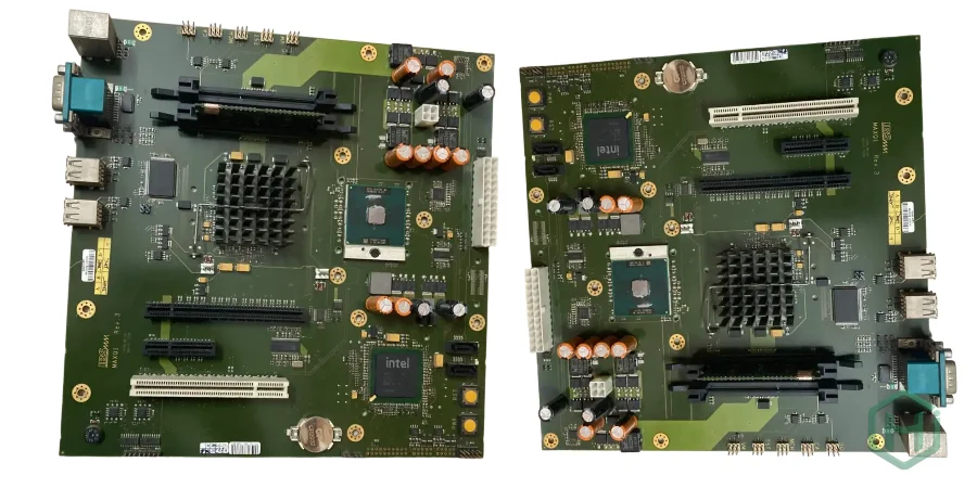
In today's highly digitized medical field, the security of patient data is as important as the accuracy of diagnoses. From high-end carts in hospital ultrasound rooms to portable, wearable monitoring patches used at home, medical devices constantly collect, process, and transmit highly sensitive personal health information (PHI). As the critical link connecting sensors to processing units, the Ultrasound probe interface PCB is no longer just a carrier of signals; it constitutes the first physical line of defense for hardware security and data privacy.
This article provides an in-depth Ultrasound probe interface PCB guide, moving beyond traditional signal integrity discussions to focus on how to build a robust hardware security architecture from the PCB design level. We will explore key technologies such as Secure Boot, data stream encryption, and physical anti-tampering, analyzing how to weave security genes into every inch of a high-speed Ultrasound probe interface PCB to achieve uncompromising Ultrasound probe interface PCB quality.
Secure Boot and Root of Trust: The starting point of the trust chain
The first step in hardware security is ensuring that the device runs only authorized and untampered software. This relies on the Secure Boot mechanism and a Hardware Root of Trust.
- Secure Boot Process: When the ultrasound device powers on, the processor does not immediately execute the main operating system. Instead, it starts from a ROM code that cannot be modified. This code verifies the digital signature of the Bootloader using public keys stored in OTP (One-Time Programmable) memory or a Secure Element. This verification chain continues—Bootloader verifies the OS, OS verifies the application—ensuring that every line of code executed has been authorized by the manufacturer.
- Hardware Root of Trust: The foundation of the entire verification chain is the physical security of the keys. In Ultrasound probe interface PCB design, a dedicated hardware security module (like TPM or Secure Element) is typically required to store these critical keys. These chips must be physically protected on the PCB layout. For instance, their communication traces with the main processor should be routed on inner layers to prevent probing and logical analyzers from stealing key data during the boot process.
Securing the data stream: From analog front-end to high-speed transmission
An ultrasound probe generates massive amounts of analog signals that are converted into digital data streams by the Analog-to-Digital Converter (ADC). Protecting these data streams from interception or tampering is a core aspect of Ultrasound probe interface PCB quality.
- Encryption at the edge: Modern secure medical device designs push encryption as close to the data source as possible. Rather than sending raw data to the main processor for encryption, the data is encrypted directly at the Analog Front-End (AFE) or within an FPGA on the interface board. This ensures that data transmitted over internal cables or wireless links is already ciphered, minimizing the attack surface.
- High-Speed interface security: The encrypted data stream is often transmitted to the host via high-speed interfaces like PCIe or USB 3.0. While these protocols have their own security mechanisms, at the physical PCB level, preventing EMI/RFI (Electromagnetic Interference/Radio Frequency Interference) leakage is crucial. Attackers can potentially reconstruct data by analyzing electromagnetic radiation (Side-Channel Attack). Therefore, a
high-speed Ultrasound probe interface PCBrequires rigorous shielding design, including a complete ground plane, optimized differential pair routing, and necessary metal shielding cans.
Physical anti-tamper design: Defending against hardware-level attacks
Software encryption alone cannot thwart an attacker with physical access to the device. A high-quality medical PCB must incorporate physical anti-tamper mechanisms.
- Active Mesh and encapsulation: For components containing highly sensitive data (like encryption chips and memories), an active mesh can be designed on the outer layers of the PCB. This mesh continuously monitors for continuity. If an attacker attempts to drill, cut, or use chemical solvents to expose the inner layers, the mesh will break, immediately triggering the security chip to erase all keys and sensitive data. Combining this with potting compounds (epoxy resin) further increases the difficulty of physical dissection.
- Tamper switches and sensors: The PCB can integrate micro-switches or light sensors. If the device enclosure is unauthorizedly opened, the change in state immediately triggers a security response, shutting down the system or erasing data.
High-performance design support: Ensuring security doesn't compromise performance
Implementing these complex security mechanisms must not come at the expense of the ultrasound device's core performance—image quality and frame rate. This places extreme demands on PCB design and manufacturing.
- Signal Integrity (SI): Strict impedance control is mandatory when designing high-speed differential pairs. This requires an accurate
Ultrasound probe interface PCB stackupmodel, verified via simulation tools like impedance calculators. Length matching, optimized via design (like backdrilling), and rational routing topologies are all key to minimizing reflections and crosstalk. - Power Integrity (PI): Security chips and high-speed processors demand exceptionally clean power. The PCB design must suppress power supply noise by placing an adequate number and value of decoupling capacitors and building a low-impedance Power Delivery Network (PDN). For projects requiring rapid prototype validation, choosing a reliable
Ultrasound probe interface PCB quick turnservice is vital; it accelerates product iteration without sacrificing SI/PI performance. HILPCB's High-Speed PCB manufacturing capabilities ensure consistency and high performance from prototype to mass production.
🏥 Medical Device PCBs: Hardware Security and Compliance Design Framework
Physical layer security and data privacy protection based on IEC 60601-1 standards
Security Guideline: Place the TPM/Secure Element in the central area of the PCB and utilize buried routing. Maintain keep-out zones around it to prevent the extraction of key information via Side-Channel Analysis (SCA).
Compliance Guideline: Strictly enforce creepage distances required by Means of Patient Protection (MOPP). Utilize full-coverage ground planes (GND Plane) within the stackup to provide dual electromagnetic and physical isolation for sensitive medical signals.
Security Guideline: Cover critical areas with an Active Mesh. Combined with a potting process, this ensures that under violent disassembly or micro-drilling attacks, the security chip instantly triggers self-destruct logic to erase keys.
Performance Guideline: Provide a dedicated LDO power plane for the security processor. Utilize embedded capacitance to lower internal power resistance, ensuring power transients during cryptographic operations do not impact the performance of highly sensitive front-end sensors.
Regulatory Roadmap and Supply Chain Security: Meeting global medical compliance requirements
The design and manufacturing of medical devices are subject to strict regulatory oversight globally, such as the FDA in the US and the MDR in the EU. These regulations focus not only on clinical efficacy and biocompatibility but increasingly emphasize cybersecurity and data privacy. A comprehensive Ultrasound probe interface PCB guide must include a detailed compliance checklist to ensure the PCB design, materials, and manufacturing processes meet target market regulations.
For example, material traceability is a fundamental requirement in medical device manufacturing. The base materials used for the PCB (e.g., FR-4, Rogers), solder mask inks, and surface finishes must have clear source records and comply with environmental directives like RoHS. Components coming into direct or indirect contact with the human body also require biocompatibility testing (e.g., ISO 10993).
Supply chain security is another critical aspect of compliance. Selecting a trustworthy PCB supplier is paramount. You must ensure the supplier has secure manufacturing facilities, can protect your IP (Intellectual Property) from leakage, and implements strict quality control and security protocols during production. This is especially critical during the Ultrasound probe interface PCB mass production phase; quality deviations in any batch can lead to product recalls and massive compliance risks. Whether for rapid iteration using an Ultrasound probe interface PCB quick turn service or for large-scale production, choosing a partner like HILPCB, which holds ISO 13485 (Medical Device Quality Management System) certification, can greatly simplify your compliance process. Our advanced manufacturing capabilities, such as HDI PCB technology, also open possibilities for designing smaller, more secure portable medical devices.
FAQ
Why is Secure Boot important on an ultrasound probe interface PCB?
Because it ensures the device starts only with authenticated firmware. That trust chain helps prevent tampered bootloaders, operating systems, or applications from accessing protected medical data.
Where should security keys and trust anchors be protected on the PCB?
They should be stored in dedicated hardware such as a TPM or Secure Element and placed in a physically protected layout area. Routing the related traces on inner layers also reduces exposure to probing and side-channel attacks.
Why should data be encrypted close to the analog front-end?
Encrypting data near the source reduces the amount of raw patient data exposed on internal links. That makes cables, connectors, and downstream interconnects less attractive attack points.
Which physical anti-tamper methods are practical for this type of medical board?
Common measures include active mesh structures, potting compounds, tamper switches, and light sensors. These features help detect physical intrusion and trigger protective actions such as shutdown or key erasure.
Conclusion: Embedding security into every inch of PCB design
In conclusion, Ultrasound probe interface PCB quality is a comprehensive concept extending far beyond traditional electrical performance. As the first gateway for medical data security, it demands that security thinking be embedded into every stage of design. From establishing a chain of trust via Secure Boot and protecting data flows with encryption technologies, to implementing physical anti-tamper measures, the realization of every security function is inextricably linked to the underlying support of a high-quality PCB.
A successful high-speed Ultrasound probe interface PCB project requires tight collaboration between design engineers and PCB manufacturers to jointly establish a comprehensive Ultrasound probe interface PCB guide. This guide must focus not only on signal and power integrity but must also place data security, physical protection, and regulatory compliance at its core. By selecting an experienced, technologically advanced, and security-focused partner, you can ensure your medical devices provide uncompromising data privacy protection for patients, starting from the foundational PCB level.