
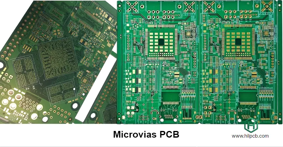
As artificial intelligence, particularly large language models (LLMs), experiences explosive growth, the hardware driving these algorithms—AI accelerator chips (like GPUs, TPUs, and specialized ASICs)—is undergoing an unprecedented evolution. These chips are characterized by massive transistor counts, ultra-high computational density, and enormous power consumption. To integrate these "monsters" onto a PCB, traditional packaging and interconnect technologies have reached their physical limits.
The core challenge lies in the I/O pin density. Modern AI chips utilize ultra-fine pitch Ball Grid Arrays (BGAs), where thousands of pins are packed into a very small area. Traditional "dog-bone" fan-out routing methods simply cannot extract signals from the inner rows of these high-density BGAs. This is where Via-in-Pad plated over (VIPPO) technology comes into play, transitioning from an advanced option to an absolute necessity.
This article provides an in-depth analysis of VIPPO technology, exploring its fundamental principles and demonstrating how it solves the trio of interconnect, signal integrity, and thermal management bottlenecks in AI chip packaging.
What is Via-in-Pad plated over (VIPPO)?
Traditionally, vias (the holes connecting different PCB layers) were placed adjacent to component pads, connected by a short trace. However, as components shrink, this short trace and the via itself consume valuable surface routing space.
Via-in-Pad plated over (VIPPO), also known as POFV (Pad on Filled Via), revolutionizes this structure. The process involves:
- Drilling: Drilling the via directly within the surface pad.
- Plating: Plating the via walls with copper to establish electrical connections between layers.
- Filling: Filling the via hole completely with a special epoxy resin (either conductive or non-conductive).
- Planarization: Grinding the surface flat.
- Capping: Plating a solid copper "cap" over the filled via, creating a completely flat, solderable surface pad.
The result is a pad that looks identical to a standard solid pad from the outside, but hides a vertical interconnect channel beneath it. This structure brings revolutionary advantages for high-density BGA fan-out.
Why do AI chips desperately need VIPPO?
AI chip carrier boards and the main server motherboards they attach to face extreme design constraints. Via-in-Pad plated over (VIPPO) offers perfect solutions to these constraints:
1. Extreme routing density and BGA fan-out
For a BGA with a 0.8mm or even 0.5mm pitch, there is simply no physical space to route traces from the inner pins to the outside on the surface layer. By placing vias directly in the pads, VIPPO allows signals from every BGA pin to dive directly to the inner layers of the PCB. This "vertical fan-out" strategy instantly frees up massive amounts of routing space on the surface and inner layers, enabling the layout of highly complex multi-layer boards.
2. Enhancing Signal Integrity (SI) and Power Integrity (PI)
AI chips require extremely high bandwidth, often utilizing PCIe Gen 5/6 or proprietary high-speed interconnects (like NVLink).
- Shorter Signal Paths: VIPPO eliminates the parasitic inductance and capacitance introduced by the surface trace connecting the pad to a traditional via. For high-speed signals, every millimeter counts. A direct vertical path significantly reduces signal reflection and insertion loss.
- Lower PDN Impedance: AI chips can experience transient currents of hundreds of amperes. VIPPO allows decoupling capacitors to be placed directly underneath the BGA on the opposite side of the board, using vias directly in the capacitor pads. This creates the shortest possible current loop, drastically reducing the impedance of the Power Delivery Network (PDN) and ensuring stable power supply during high-frequency switching.
3. Superior Thermal Management Capabilities
The power consumption of top-tier AI chips has surpassed 1000W. Heat dissipation is a matter of life and death. VIPPO naturally functions as a thermal via array. Heat generated by the chip transfers directly from the solder bumps into the copper cap of the VIPPO pad, and then conducts down the copper-plated via walls directly to the internal large-area ground planes or a backside heatsink. Compared to the poor thermal conductivity of standard FR-4 substrate, this direct copper thermal path increases heat dissipation efficiency exponentially.
🎯 VIPPO Process: Key Checkpoints for High-Density Design & Manufacturing
Core manufacturing guidelines for optimizing BGA fan-out density and signal integrity
Engineering Guideline: It is imperative to ensure the resin filling is completely dense. Residual air bubbles will expand violently under the high temperatures of reflow soldering, leading to pad lifting or solder joint cracking, directly threatening the long-term reliability of the BGA connection.
Engineering Guideline: The flatness of the plated cap directly determines the soldering yield. Copper reduction and polishing processes must be strictly controlled to ensure pad surface dimples or protrusions are kept within minimal tolerances, avoiding cold joints or the Head-in-Pillow (HoP) defect.
Engineering Guideline: Vias with a high Aspect Ratio significantly increase the difficulty of chemical penetration and resin filling. For thick board designs, vacuum pressure filling parameters must be confirmed with the manufacturer in advance to prevent insufficient filling inside the hole.
Engineering Guideline: Due to the added steps of filling, planarization, and secondary plating, VIPPO comes at a premium. It is recommended to use it selectively only in the core areas of BGAs with pitches below 0.8mm, or in transition zones with extreme demands for thermal dissipation or signal return paths.
How does VIPPO synergize with advanced packaging technologies (like Copper Pillar)?
Advanced packaging technologies, such as 2.5D/3D packaging (CoWoS, Foveros, etc.), are key to sustaining Moore's Law. In these technologies, chips are no longer isolated entities but are integrated into a highly complex System-in-Package (SiP) via high-density interposers or direct bonding. Via-in-Pad plated over (VIPPO) acts as the vital bridge connecting these complex packages to the main PCB.
The value of VIPPO is particularly evident when combined with Copper pillar bump technology. Compared to traditional solder bumps, Copper pillar offers lower electrical resistance, superior current-carrying capacity, and better thermal performance, making it the preferred choice for high-performance flip-chip designs. The extremely fine pitch of these copper pillars places incredibly high demands on substrate pad density and precision.
Via-in-Pad plated over (VIPPO) technology can create perfectly flat, high-density pads on the IC substrate that precisely match the Copper pillar array. This direct "pillar-to-pad" connection establishes a seamless, high-performance electrical and thermal conduit from the chip to the PCB. This synergy is especially critical for integrating High Bandwidth Memory (HBM). HBM connects to the processor through thousands of microscopic interconnect channels; even minor impedance mismatches or path length discrepancies can cause data transmission errors. VIPPO ensures the uniformity and consistency of these channels at the substrate level, which is crucial for achieving High-Speed PCB design goals.
How to balance the performance advantages of VIPPO with manufacturing costs?
Without a doubt, Via-in-Pad plated over (VIPPO) is a value-added process; its cost is higher than standard via technology. The cost increase primarily stems from additional materials (filling resin) and extra processing steps (filling, planarization, secondary plating). Therefore, using VIPPO judiciously in your design is key to achieving cost-effectiveness.
An effective design strategy is regional application. Not every component on the board requires VIPPO. Designers should restrict its use to areas where it is truly necessary, such as ultra-fine pitch BGAs, fan-out regions for high-speed interfaces, and directly beneath critical components requiring enhanced thermal dissipation. For other non-critical areas, lower-cost traditional via technologies can still be employed.
Collaborating with an experienced PCB manufacturer is paramount. A manufacturer like HILPCB can provide professional DFM (Design for Manufacturability) feedback. Early in the design phase, our engineering team can review your layout and advise where using VIPPO will yield the maximum performance return, and where alternative solutions (like microvias) can be used to reduce costs. For example, in certain Hybrid stack-up (Rogers+FR-4) designs, we can help you optimize the via strategy across different material zones to strike the optimal balance between performance and budget. For designs demanding extreme density, our HDI PCB manufacturing capabilities provide a comprehensive suite of solutions, including VIPPO.
Common Questions
Why has VIPPO become necessary for modern AI chip boards instead of optional?
Because ultra-fine-pitch BGAs leave too little room for traditional dog-bone fan-out routing. VIPPO lets each pad drop signals vertically into inner layers, which makes extreme I/O density practical and frees routing space for complex AI accelerator boards.
How does VIPPO improve signal integrity, power delivery, and thermal performance?
It removes the extra pad-to-via trace, reducing parasitic inductance and capacitance on critical signals. It also lets decoupling capacitors sit directly under the BGA to lower PDN impedance, while the copper-filled vertical path works as a thermal conduit that pushes heat into internal planes or heatsinks.
How should teams control VIPPO cost and manufacturing risk?
The safest approach is to use VIPPO only in areas that truly need density, return-path quality, or thermal extraction. Designers should also confirm void-free filling, flat cap plating, aspect-ratio limits, and DFM review details with an experienced manufacturer so VIPPO is applied where it delivers the highest return.
Conclusion: VIPPO is the obligatory path to future AI hardware
Via-in-Pad plated over (VIPPO) technology has evolved from a "nice-to-have" option into a core enabling technology driving the development of next-generation AI and high-performance computing hardware. By providing unparalleled routing density, superior signal integrity, efficient thermal pathways, and stable power delivery, it directly addresses the myriad challenges posed by AI chips. Fundamentally, without VIPPO, the complex designs of modern AI accelerator carrier boards would be nearly impossible to realize.
However, fully unlocking the potential of Via-in-Pad plated over (VIPPO) requires tight, synergistic collaboration between design engineers and manufacturers. A profound understanding of its design rules, manufacturing limitations, and quality control checkpoints is a prerequisite for project success. Choosing a partner like HILPCB, with its deep technical expertise and advanced process capabilities, ensures a seamless transition for your next-generation AI products from design concept to final physical reality. Our precise mastery of Controlled impedance, extensive experience with Heavy copper 3oz+ processing, and deep understanding of advanced packaging interfaces like Copper pillar will provide a rock-solid manufacturing foundation for your innovations.