
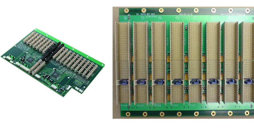
Backplane PCBs connect boards, modules and connectors in larger electronic systems. They may need high layer counts, controlled interconnect loss and tight mechanical tolerances, but the exact requirements depend on the bus, connector system and deployment environment. HILPCB can review the manufacturing requirements of customer-supplied designs.
Related services include backplane PCBs, HDI PCBs and high-Tg materials. IC package substrates are a different fabrication category and should not be treated as interchangeable with system backplanes.
What Defines a Manufacturable Backplane?
For a custom backplane PCB, confirm the interconnect architecture before selecting layer count or material. A passive backplane primarily routes signals and power between modules; an active backplane may include switching or other circuitry. Connector density, channel length, power distribution and mechanical support drive different fabrication and assembly requirements.
| Design area | Inputs needed | Review and evidence |
|---|---|---|
| Size and construction | Outline, thickness, layer stack, copper distribution and support points | Build-specific panel feasibility, registration and bow/twist limits |
| Signal channels | Interface, lane rate, length, connector/launch models and receiver budget | Loss, impedance, crosstalk and return-path assessment of the complete channel |
| Material | Exact laminate/prepreg grade, construction, copper foil and frequency-dependent properties | Approved stackup and substitution rules; a brand or high-Tg label alone does not establish channel margin |
| Via strategy | Through, blind/buried or microvia structures; required backdrill and residual stub | Drill capability, aspect ratio, registration and test/coupon requirements |
| Connector mechanics | Approved footprint, mounting hardware, mating forces and chassis datum scheme | Hole/position tolerances, connector fit and assembly support |
| Power distribution | Continuous/transient current, terminals, cooling and allowable temperature rise | Copper, vias, contacts and temperature validation for the intended load |
A 64-layer count, extra thickness or heavy copper is not a default requirement or an automatically available combination. Confirm the actual construction and quantity with the fabricator.
Press-Fit Holes Need Connector-Specific Requirements
A compliant press-fit contact depends on the finished plated hole and the specified contact working together. Obtain the connector manufacturer's current application specification: finished-hole diameter and tolerance, plating, board thickness, pad geometry and insertion process may all matter. Drill diameter is not interchangeable with finished-hole diameter.
Agree hole inspection, board support, insertion tooling and acceptance evidence before assembly. Excessive insertion force or an unsuitable hole can damage the barrel or contact. A backdrill must not remove the required contact engagement region; coordinate stub removal with the connector and board design. Gold fingers and bevels are separate edge-interface features, not substitutes for press-fit hole control.
Material and Channel Choices Follow the Actual Interface
PCIe, Ethernet, proprietary serial links and control buses need their own channel requirements. A connector's nominal speed or material-family label does not establish end-to-end performance. Evaluate frequency-dependent loss, trace geometry, copper roughness, launches, vias and connector transitions together. Choose low-loss material only where the channel budget justifies it and the resulting fabrication process is compatible.
Polyimide, high-Tg FR-4, Panasonic Megtron grades and Rogers grades differ in properties and processing; they are not interchangeable options for every backplane. Agree exact grades and any hybrid construction rather than selecting from a generic family list.
Assembly and Handling Scope
HILPCB offers custom backplane PCB fabrication and assembly. Depending on the quoted construction, capability includes 18–64 layers, tight registration, boards 2 mm or thicker, with heavy-copper options specified separately by copper weight, long formats, and high-Tg FR-4, polyimide, Megtron 6 or Rogers 4350B. Options include sequential lamination, backdrilling, blind/buried vias, controlled-depth drilling, epoxy plugging, gold fingers and beveling; interface-specific builds can support PCIe, XAUI, USB, DDR4 or custom buses. Assembly can cover large or heavy boards with BGA, press-fit and through-hole connectors, AOI and optional ICT. ESD packaging, international shipping, flexible invoicing and secure payment options are available. Qualified 5–8-working-day fabrication, impedance/thermal reviews, layer/X-ray/AOI reports, and material/batch traceability can be quoted. These maxima need not combine in one build; connector/channel release requirements need review, and this is not package-substrate fabrication.
A backplane can be largely passive or carry numerous populated circuits. For backplane PCB assembly, submit the BOM, connector list, placement and insertion instructions, test access and mechanical support requirements. Confirm the board size/weight, component packages, press-fit or through-hole processes and any required fixtures with the supplier.
Agree AOI, connector inspection, continuity and any ICT/functional tests according to actual defect risks and accessibility. Define ESD and mechanical packaging to protect connectors and prevent board flex during handling. Shipping, destination requirements and payment terms belong in the quotation rather than serving as evidence of technical capability.
Before fabrication, inspect Gerbers in the Gerber Viewer and validate stack-up, drill, connector footprint and mechanical CAD using suitable engineering tools. A visual viewer alone does not verify electrical connectivity or connector fit.
What Should Be Agreed Before Release?
| Release item | Required agreement |
|---|---|
| Fabrication files | Stackup, impedance nets/coupons, hole table, backdrill and mechanical tolerances |
| Connector acceptance | Finished-hole requirements, insertion process and agreed fit/inspection records |
| Test coverage | Bare-board electrical test, selected dimensional/microsection checks and assembly tests |
| Traceability | Material lots, board revisions and records linked to the agreed lot or unit level |
| Schedule | Material/tooling availability, first-article review, fabrication, assembly and delivery milestones |
Expedited work depends on the actual build and inspection scope. Obtain a written schedule after feasibility review; a requested lead time is not a manufacturing guarantee.
Conclusion
Backplane reliability depends on the released stackup, interconnect channel, connector interface and mechanical installation working together. Send HILPCB the relevant design files and acceptance requirements, then confirm which fabrication, assembly and test services are feasible for the build.
Use HDI PCBs where density warrants them and select high-Tg laminates against the actual thermal and process requirements. IC substrate integration is a separate package-level scope; it should not be inferred from a system-backplane quotation.