
Writing "Include standard test coupons" in a PCB fabrication note leaves the most important quality and procurement variables undefined: which physical structures are placed on the production panel rails, which test procedures are run on them, and what numerical acceptance criteria govern shipment release. Because you cannot saw a customer-shipping board in half to measure inner-layer plating thickness—and you cannot land a high-frequency coaxial TDR probe cleanly on a dense BGA breakout trace loaded with stubs—test coupons serve as purpose-built sacrificial proxies manufactured on the same panel as the product boards.
To make coupon data actionable during incoming quality inspection (IQC), each coupon must match the exact layer stack, hole aspect ratio, or conductor geometry of the product board, and every lab report must tie its serial ID back to the specific manufacturing panel and lot. For detailed TDR waveform setup and impedance calculation, see our PCB impedance testing guide.
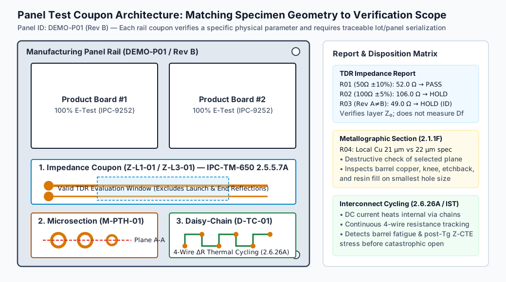
1. Matching Coupon Architecture to the Engineering Verification Task
A single coupon geometry cannot validate electrical impedance, hole-wall metallurgy, and long-term thermal cycling simultaneously. Before panelization freezes, map each project verification requirement to its dedicated coupon structure and governing IPC-TM-650 test method:
| Verification Objective | Panel Coupon Structure | Governing Method Basis | What the Coupon Measures | What Passing Does Not Prove |
|---|---|---|---|---|
| Controlled Impedance (Z0 / Zdiff) | Layer-specific single-ended and differential transmission lines with dedicated GND-Signal probe launches | IPC-TM-650 2.5.5.7A; Polar AP8525 | Characteristic impedance over a defined uniform line window after etching, lamination, and solder-mask application | Full-channel insertion loss (S21), laminate Df, or connector/via-transition discontinuities on the product board |
| PTH / Microvia Metallurgy & Laminate Integrity | Metallographic cross-section coupon (or sacrificial product board) containing the smallest drill sizes and via stacks | IPC-TM-650 2.1.1F (preparation) + IPC-TM-650 2.6.8E (thermal stress) | Barrel copper thickness, knee wrap, inner-layer foil connection (etchback/smear), resin fill, and post-thermal-shock delamination | 100% netlist continuity across all holes on the shipping boards (requires IPC-9252 electrical test) |
| Interconnect Thermal-Cycling Endurance | Stitched 4-wire Kelvin daisy-chain coupon cycling through target via spans | IPC-TM-650 2.6.26A (DC current-induced cycling / IST) | Resistance drift (Δ R) under repeated thermomechanical Z-axis expansion cycles past laminate Tg | Unconditional field service lifetime in years without an application-specific acceleration model |
| Surface Cleanliness / Solderability / Peel | Dedicated comb-pattern (SIR), unpopulated surface-finish pads, or peel-strip specimens | IPC-TM-650 2.3.25 (ROSE), 2.6.3.7 (SIR), J-STD-003 | Ionic contamination equivalent, insulation resistance under humidity bias, or initial pad wetting | Post-SMT assembly cleanliness after customer reflow or hand rework |
(Downloadable planning matrix: specimen-selection-and-quote.csv.)
Note that IPC-TM-650 2.1.1 Revision F explicitly permits metallographic microsections to be taken from either a dedicated test coupon or an actual printed board containing the features of interest, and notes that multiple section planes may be required when different hole families (such as through-holes, blind laser microvias, and buried core vias) exist in the same stackup.
2. Three Technical Requirements That Determine Coupon Representativeness
A coupon sharing the same panel border as your PCB can still produce misleading results if its local geometry or measurement setup diverges from the product board:
A. Impedance Coupons: Coating State and the TDR Evaluation Window
When a TDR step generator injects a fast edge into an impedance coupon, the initial part of the waveform includes inductive/capacitive aberrations from the probe tips and launch pads, while the far end reflects off the open termination. As illustrated in Polar Instruments Application Note AP8525, the test program must define a stable evaluation window (commonly 20% to 80% of the coupon trace length, or a specified time window in picoseconds) that excludes launch and end effects without selectively cropping out real mid-line impedance dips.
Equally important is surface condition parity (Polar AP8502): if outer-layer controlled-impedance microstrip lines on the product board are covered with liquid photoimageable (LPI) solder mask—which typically lowers single-ended impedance by 2--3 Ω—the impedance coupon trace must receive the exact same solder-mask coating.
B. Microsection Coupons: Smallest Drill Diameter and Plane A–A Accuracy
Electroplating throwing power is lowest inside the highest-aspect-ratio (smallest diameter, deepest span) holes. If your board contains 0.15 mm mechanical vias alongside 0.80 mm connector holes, a microsection coupon that only sections 0.50 mm holes cannot verify barrel copper thickness in the 0.15 mm vias. Furthermore, during manual or semi-automatic grinding (IPC-TM-650 2.1.1F), the polish plane (Plane A–A) must intersect within ± 10% of the true hole center diameter; under-polishing or over-polishing off-center distorts apparent wall thickness and hides inner-layer foil separation.
C. Daisy-Chain Thermal Cycling: Capturing Post-Tg Z-Axis Expansion
In IPC-TM-650 2.6.26A (DC current-induced thermal cycling / IST), direct current heats internal interconnect chains between ambient temperature and assembly/stress temperatures while a 4-wire Kelvin bridge continuously tracks resistance change (Δ R). Above the laminate glass-transition temperature (Tg), Z-axis thermal expansion jumps sharply (for example, from ~45 ppm/°C pre-Tg to >200 ppm/°C post-Tg in standard high-Tg epoxies), pulling vertically on plated via barrels and microvia-to-target interfaces. Section 5.1.2 of the method distinguishes random sampling, selective sampling (targeting high-risk panel zones), and comparative sampling across process lots—making coupon location and copper density critical when comparing two laminate systems.
3. Worked Report Audit: Separating Identity, Measurement, and Disposition
When reviewing incoming supplier coupon reports, audit specimen identity and revision, measured values against the contracted window, and nonconformance disposition independently. A green "PASS" stamp on a summary sheet does not override an out-of-spec line item or a mismatched revision.
Consider four coupon records submitted for panel P01 of order DEMO-100 (contracted to Revision B, with project requirements of 50 Ω ± 10% single-ended, 100 Ω ± 5% differential, and a drawing callout of ≥ 22 μm minimum local PTH barrel copper):
| Record ID | Order / Rev | Panel / Coupon ID | Verification Test | Contracted Acceptance Window | Reported Result | Engineering Audit & Disposition |
|---|---|---|---|---|---|---|
| R01 | DEMO-100 / Rev B | P01 / Z-L1-01 |
L1 Single-Ended TDR (IPC-TM-650 2.5.5.7A) | 50 Ω ± 10% (45.0--55.0 Ω) | 52.0 Ω | PASS — Matches Rev B identity and sits within the 45.0--55.0 Ω window |
| R02 | DEMO-100 / Rev B | P01 / Z-L3-01 |
L3 Differential TDR (IPC-TM-650 2.5.5.7A) | 100 Ω ± 5% (95.0--105.0 Ω) | 106.0 Ω | HOLD (Out of Spec) — Exceeds 105.0 Ω upper limit by +1.0 Ω; cannot be waived by R01 passing |
| R03 | DEMO-100 / Rev A | P01 / Z-L1-01 |
L1 Single-Ended TDR | 50 Ω ± 10% (45.0--55.0 Ω) | 49.0 Ω | HOLD (Revision Mismatch) — Value is within band, but test program/coupon references superseded Rev A stackup |
| R04 | DEMO-100 / Rev B | P01 / M-PTH-01 |
PTH Cross-Section (IPC-TM-650 2.1.1F) | Drawing callout: local barrel Cu ≥ 22 μm | 21 µm | HOLD (Below Drawing Spec) — Meets standard Class 2 20 μm average, but falls 1 μm below customer drawing callout |
(Downloadable report audit dataset: illustrative-report-results.csv and notes.)
How to Investigate and Close Each Hold Without Losing Traceability
- Closing
R02(106.0 Ω Differential TDR Hold): Do not silently re-probe the coupon with a narrower evaluation window just to hunt for a number below 105.0 Ω. First verify probe polarity, calibration standard, and whether the measurement included a launch reflection. Next, cross-check the L3 microsection (M-PTH-01) to see if pressed prepreg thickness came out thicker than nominal or if L3 trace width was over-etched. If the physical board truly sits at 106.0 Ω, the design/SI authority must decide whether to grant a lot-specific engineering concession (MRB waiver) or reject the affected panel(s), preserving the originalR02log alongside the disposition. - Closing
R03(Revision A vs. Revision B Mismatch): An in-band impedance number (49.0 Ω) is invalid if the operator loaded the Revision A TDR test recipe or if CAM stepped an outdated Revision A coupon onto a Revision B panel. Quarantine the lot until CAM confirms whether the physical panel etched Revision B artwork (requiring only a corrected test-program header and re-test) or Revision A artwork (requiring lot rejection). - Closing
R04(21 µm Barrel Copper vs. 22 µm Drawing Spec): Verify measurement uncertainty on the optical/SEM microscope, check the other five wall measurement zones in the section, and section a backup coupon from the center and corner of panelP01to establish whether plating thickness was low across the bath load or localized to one rail position.
4. Procurement Cost Drivers and Panel Utilization Tradeoffs
Adding custom coupons and laboratory reports affects quotation scope in four concrete ways that procurement should normalize across competing suppliers:
- Panel Border Utilization: Standard impedance and microsection coupons fit within routine 10--20 mm manufacturing rails. Long differential insertion-loss coupons (such as 100--150 mm SET2DIL / VNA structures) or large IST daisy-chain coupons consume active panel area and can reduce the number of shipping boards per panel.
- Sampling Frequency (Per-Lot vs. Per-Panel): Specifying 100% per-panel TDR testing and per-panel microsectioning provides panel-level isolation if one press opening or plating rack drifts, whereas lot-level sampling (e.g., 1–2 panels per batch) lowers lab labor cost for stable repeat builds.
- Conditioning Protocol Before Sectioning: Evaluating an as-fabricated microsection is faster than running 3× or 6× solder-float thermal shock (IPC-TM-650 2.6.8E at 288°C for 10 s) or convection reflow simulation (IPC-9631 / 2.6.27) prior to potting and polishing.
- Physical Mount & Coupon Retention: Specify whether cured epoxy microsection pucks, remaining unsectioned coupons, and raw
.csv/ TDR waveform files must ship in the box with the PCBs or remain archived at the factory for a defined retention period.
5. RFQ Checklist for PCB Test Coupons and Quality Deliverables
When submitting a controlled-impedance design review or PCB manufacturing inquiry, include these fields in your fabrication drawing and PO notes:
- Coupon Types Required: Explicitly call out TDR impedance coupons (listing every controlled layer, trace width/space, reference planes, and target Ω ± %), metallographic microsection coupons (covering the smallest PTH, blind/buried vias, and VIPPO structures), and any thermal-cycling or cleanliness specimens.
- Serialization & Traceability: Require each board and its corresponding panel coupons to share a laser-marked or etched Panel ID (
Panel #01,Panel #02, etc.) so a failing coupon isolates the exact affected boards rather than placing the entire production lot in blind quarantine. - Test Standards & Conditioning: State the governing standard and revision (e.g., IPC-6012 Class 2 or Class 3, IPC-TM-650 2.5.5.7A for TDR, IPC-TM-650 2.6.8E Condition A for thermal stress).
- Deliverable Package: Specify high-resolution annotated microsection micrographs (with scale bars and measured copper/dielectric dimensions), TDR waveform plots showing the evaluation window, and raw pass/fail data tables.
HILPCB provides in-house TDR impedance verification (supporting ±10% standard and ±5% advanced tolerances), sample-based VNA S-parameter testing up to 40 GHz, metallographic cross-section analysis, thermal-stress testing, and IST interconnect cycling (200–500 cycles) across our multilayer PCB and HDI PCB lines. Upload your Gerber files and stackup requirements when you request a quote to lock your coupon layout and inspection deliverables before panelization.
Frequently Asked Questions
Does a passing TDR impedance coupon prove my high-speed channel will pass insertion-loss requirements?
No. A standard TDR coupon (IPC-TM-650 2.5.5.7A) verifies characteristic impedance (Z0 or Zdiff) determined primarily by trace width, dielectric thickness, and real permittivity (Dk). It does not measure dielectric loss tangent (Df) or high-frequency copper roughness loss, which require broadband VNA S-parameter (S21) or differential phase/loss test structures.
Why must panel coupons be serialized to individual manufacturing panels?
Lamination press pressure, copper electroplating current density, and etching uniformity can vary from panel to panel across a production lot. If coupons and shipping boards are stamped with matching panel numbers (P01, P02, etc.), an out-of-spec TDR or microsection result on P02 allows quality engineering to quarantine or disposition P02 specifically—and verify whether neighboring panels are affected—rather than losing traceability across the entire shipment.
Can the fabricator place microsection and impedance coupons on the breakaway panel rails?
Yes, placing coupons on the manufacturing panel rails (or customer sub-panel rails) is standard practice because those zones experience the same lamination press cycle, drilling setup, plating bath, and etching line as the product boards without consuming finished board area. For large panels or critical Class 3 builds, diagonally opposite rail coupons (e.g., diagonally at two panel corners) are commonly used to capture center-to-edge plating and press-thickness gradients.
Should solder mask be applied over outer-layer impedance coupon traces?
The coupon must match the finished product board. If your outer-layer controlled-impedance microstrip traces are covered by solder mask on the PCB, the corresponding coupon traces must also be coated with the same solder mask. Leaving the coupon trace bare air-microstrip while coating the product board will make the coupon read 2--3 Ω higher than the actual traces on the shipped PCB.