
When post-reflow AOI flags a solder bridge across two adjacent SMT leads on a 0.4 mm or 0.5 mm pitch QFP, QFN, or connector, the most common floor-level mistake is immediately shrinking the stencil thickness or dropping reflow peak temperature. A post-reflow solder bridge is only the final solidified state—the unwanted connection could have formed during stencil printing, during pick-and-place compression, or during reflow heating.
Effective prevention starts by identifying the earliest process stage where solder or paste crosses the inter-pad insulation gap, while verifying that any corrective adjustment does not starve neighboring components of solder volume. Note that this guide covers visible SMT leads and perimeter pads; for hidden array balls beneath BGAs and LGAs, use our dedicated BGA soldering defects and X-ray guide.
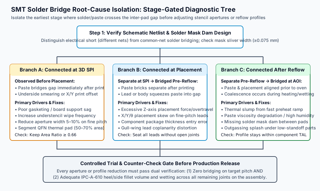
1. Gate 0: Separate Electrical Shorts from Common-Net Workmanship Bridges
Before modifying stencil apertures or printer parameters, inspect the bridged pin pair against the released CAD schematic netlist and solder-mask artwork:
- Different Nets (True Electrical Short): If Pin 14 (
VCC) and Pin 15 (GNDorSDA) are bridged by solder, the defect is both an IPC-A-610 workmanship reject and a hard electrical short that can damage components during power-up ICT/FCT. - Common Net (Same-Net Solder Bridge): High-current power ICs, QFN ground pins, and shielded connectors frequently assign two or more adjacent pins to the exact same net (
GNDorSW). If the PCB layout omitted the solder-mask web between those adjacent common-net pads (or tied them together with a wide copper flood between pads), molten solder will naturally coalesce across the unmasked copper.- Important Contract Boundary: Even when two bridged pins share the same electrical net and pass functional testing, unintended solder bridging across separate component leads is still flagged as a workmanship defect under IPC-A-610 unless the design drawing explicitly defines a shared/gang land pattern or a documented customer workmanship concession.
2. Locating the Earliest Stage of Bridge Formation
As documented in Kester's SMT defect minimization guidelines and Indium Corporation's reflow profile analysis, solder bridging follows three distinct physical pathways depending on when the paste or solder first makes contact across the gap. Use matched, same-field-of-view inspection images from 3D SPI, pre-reflow placement AOI, and post-reflow AOI to isolate the active branch:
(Downloadable stage-gated troubleshooting matrix: 04-solder-bridge-diagnostic.csv.)
Branch A: Paste Deposits Are Already Connected After Printing (3D SPI)
If 3D SPI shows solder paste bridging the gap between adjacent pads before a component ever touches the board, the reflow oven is innocent. Investigate four printing mechanics (detailed in our solder paste inspection (SPI) guide):
- Poor Stencil-to-PCB Gasketing: If the PCB warps downward due to insufficient under-board support pins—or if a tall nearby silkscreen legend or thick copper trace holds the stencil foil slightly off the pads—squeegee pressure pumps paste underneath the stencil web ("underside bleed").
- Infrequent Understencil Wiping: Dried or smeared paste clinging to the bottom of fine-pitch stencil webs transfers directly onto the solder mask dam on subsequent prints. Shortening the wet/vacuum/dry wipe interval (e.g., from every 10 prints to every 3–5 prints) immediately clears underside smearing.
- Print Registration Offset: A global X/Y/θ fiducial alignment shift pushes printed paste bricks off the copper pads and onto the inter-pad solder mask web, where adjacent deposits touch or slump together.
- Excessive Aperture Width on Fine Pitch: Printing 1:1 aperture-to-pad width on 0.4--0.5 mm pitch gull-wing or QFN pads leaves minimal margin for print variation. Reducing aperture width by 5–10% (while maintaining aperture area ratio AR = (W · L / 2(W+L)T) ≥ 0.66) narrows the printed brick without sacrificing vertical release consistency.
Branch B: Paste Is Separate at SPI, But Connected Immediately After Placement
When 3D SPI confirms clean, separated rectangular paste bricks, yet pre-reflow AOI shows paste squeezed across the gap after pick-and-place mounting, the cause lies in mechanical displacement during component seating:
- Excessive Nozzle Z-Axis Force / Overtravel: If the component thickness in the pick-and-place package library is entered too small—or if Z-axis placement force is set too high without spring buffering—the component leads smash the paste bricks flat, extruding wet paste sideways across the gap.
- Placement X/Y/θ Skew: Even a 0.05--0.08 mm rotational or lateral placement offset on a 0.4 mm pitch QFP places the metal lead edge into the gap between two paste deposits, creating a mechanical capillary bridge between both bricks.
- QFN / LGA Center Thermal Pad Paste Squeeze-Out: Printing a solid 100% solder paste brick on a QFN's large central exposed thermal pad causes the package to float or compress excess molten solder outward into the surrounding perimeter signal pins. Always segment large thermal-pad stencil apertures into a windowpane grid covering 50–70% of the pad area, leaving 0.25--0.40 mm web channels for flux outgassing and planar seating.
Branch C: Paste Remains Separate After Placement, But Bridges During Reflow
When pre-reflow inspection proves the paste and leads are cleanly separated entering the oven, bridging occurs through liquid-phase coalescence or thermal slump:
- Missing or Narrow Solder Mask Dams (Web Slivers): Solder mask between fine-pitch pads acts as a physical non-wetting barrier. For LPI solder mask, maintain a minimum mask dam width of ≥ 0.075--0.10 mm (3--4 mil). If CAD pad widths leave only a 0.03 mm mask sliver, the fabricator's CAM team must strip the sliver to prevent flaking, leaving bare laminate (or exposed copper) where molten solder easily coalesces.
- Thermal Slump During Preheat Ramp: Heating the assembly too rapidly during the initial preheat ramp (or using paste that has exceeded its stencil floor life or absorbed ambient humidity) causes the flux vehicle's viscosity to drop sharply before solvent evaporation completes. The softening paste slumps sideways across the gap before reaching liquidus (Indium Reflow Stages Part I).
3. Why "Use Less Solder Everywhere" Breaks Mixed-Technology Boards
A common knee-jerk proposal when fine-pitch ICs bridge is stepping down the entire stencil foil thickness (for example, changing from 0.125 mm / 5 mil to 0.080 mm / 3.2 mil across the whole panel). While thinner foil reduces paste volume on the bridging QFP, it simultaneously cuts solder volume by 36% on every large inductor, power MOSFET, and SMD connector on the board—causing open solder joints, insufficient heel fillets, and failed coplanarity on larger packages.
Before approving any corrective action, evaluate the required counter-check across the entire assembly:
| Candidate Corrective Action | When It Is Justified | Mandatory Counter-Check Before Production Sign-Off |
|---|---|---|
| Local Aperture Width Reduction (5–10%) or Staggered Tooth Pattern | Bridging restricted to specific 0.4--0.5 mm pitch QFP/QFN/connector footprints | Check that aperture Area Ratio stays ≥ 0.66 on 3D SPI and post-reflow joints meet IPC-A-610 minimum heel/side fillet height |
| Step-Down Stencil (0.125 mm main / 0.100 mm local cavity) | Mixed-technology board combining large power connectors with 0.4 mm fine-pitch or 0201/01005 parts | Verify keepout distance around the step cavity (3--5 mm) so neighbouring pads still gasket cleanly under the squeegee |
| Calibrate Placement Z-Height & Vision Alignment | Pre-reflow AOI confirms paste squeeze-out or lead skew after placement | Inspect 100% of pins on the package to confirm slightly lighter Z-force does not leave lifted/unseated leads (coplanarity opens) |
| Adjust Reflow Preheat Ramp & Soak Window | Post-placement paste is clean, but thermal slump bridges pads during oven entry | Verify with board-mounted thermocouples that peak temperature and time-above-liquidus (TAL) remain within limits for all heat-sensitive components |
| Restore Solder Mask Dam (≥ 0.075 mm) in CAD | Bare-board inspection shows missing mask webs between fine-pitch pads | Confirm updated pad width still satisfies component toe/heel land pattern requirements |
4. Worked NPI Case: Stopping Recurring Bridging Without Changing the Reflow Recipe
On a pilot run of an industrial controller board, post-reflow AOI flags recurring solder bridges between pins 22–28 on U4 (a 0.4 mm pitch, 64-pin LQFP). The line operator suggests lowering the reflow peak temperature from 242°C to 232°C.
Before touching the oven recipe—which is already optimized for a high-thermal-mass BGA (U1) on the same board—the process engineer checks the stage records for U4:
- 3D SPI Review: Shows paste bricks on
U4pins 22–28 are already touching along the inner edge of the footprint before placement, with deposit heights reading 145% of foil thickness and a -0.04 mm Y-offset. - Printer & Stencil Inspection: Reveals that an unpopulated silkscreen component outline box was printed directly between the
U4pad rows, lifting the stencil foil by 18 μm and preventing a flush gasket seal. - Controlled Fix & Verification: The team increases understencil wet-wipe frequency, applies a 0.03 mm inner-edge aperture reduction on
U4's stencil pads for the pilot lot, and issues a PCB DFM change to clip the silkscreen away from theU4pad row by ≥ 0.15 mm. On the 30-board verification run, 3D SPI confirms 100% separated paste deposits (92--104% volume) and post-reflow AOI verifies zero bridges and compliant IPC-A-610 gull-wing heel fillets—while leavingU1's BGA reflow profile completely untouched.
5. What to Submit for an SMT Assembly DFM and Bridging Review
To prevent fine-pitch solder bridging before stencils are cut, include the following in your SMT assembly package:
- Gerber / ODB++ Layers (Copper, Solder Mask, Paste, Silkscreen): Allowing CAM and SMT engineers to verify solder-mask dam widths (≥ 0.075 mm), silkscreen-to-pad clearances, and QFN thermal-pad via plugging.
- Complete BOM and Component Package Drawings: So engineering can cross-check 0.4 mm / 0.35 mm fine-pitch lead widths, QFN exposed-pad dimensions, and step-stencil requirements.
- Defect Map & Stage Evidence (For Troubleshooting Existing Builds): Provide annotated photos, designator/pin numbers, netlist status, and any available 3D SPI or AOI logs, along with 04-solder-bridge-diagnostic.csv.
HILPCB's SMT assembly and turnkey PCB assembly lines combine upfront stencil aperture DFM (including laser-cut nano-coated and step stencils, plus automated QFN windowpane segmentation) with 100% inline 3D SPI and multi-angle 2D/3D AOI to catch print and placement anomalies before boards ever enter the reflow oven. Upload your design files to request a quote and receive an engineering DFM review.
Frequently Asked Questions
What is the minimum solder mask dam (web) width needed to prevent SMT solder bridging?
For standard liquid photoimageable (LPI) green solder mask, maintain at least 0.075 mm to 0.10 mm (3--4 mil) of uninterrupted mask web between adjacent copper pads. Below 0.075 mm (or slightly wider for white/black solder masks), the thin mask sliver cannot adhere reliably during developing and will be removed by CAM, leaving bare dielectric between fine-pitch pads.
Why do QFN packages often bridge between the center thermal pad and the outer signal pins?
If the stencil aperture for the QFN's central exposed thermal pad is cut at 1:1 (100% coverage), too much solder paste is deposited underneath the package. During reflow, flux outgassing and package weight squeeze excess molten solder outward across the narrow gap into the perimeter pins. Segmenting the thermal-pad stencil aperture into a windowpane grid with 50%–70% total paste coverage prevents both perimeter bridging and package floating.
If a solder bridge connects two pins that are both grounded (same net), can it be shipped as-is?
Electrically, a bridge between two common-net GND pins will not cause a short circuit. However, under IPC-A-610 workmanship standards, an unplanned solder bridge connecting separate component leads or discrete lands is still classified as a defect unless the PCB footprint was intentionally designed as a shared gang land or the customer grants an explicit written workmanship concession.
Should operators hand-rework fine-pitch solder bridges immediately at the end of the line?
No. Always log the exact reference designator, pin pair, and panel location—and check whether 3D SPI and pre-reflow AOI images exist for that board—before touching the joint with a soldering iron and wick. Immediate unlogged touch-up destroys the physical evidence needed to correct a drifting stencil wipe cycle or placement offset, while adding localized thermal and flux-residue risks to the fine-pitch IC.