
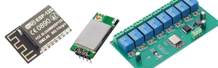
Интеграция Wi-Fi модуля на PCB — это перенос конкретной radio implementation в host product с контролируемым питанием, размещением, антенной, интерфейсами, firmware, корпусом и доказательствами соответствия. Покупка готового модуля уменьшает часть RF design, но не освобождает команду от host-layout, antenna-system, EMC, конечного изделия и production-test решений.
Главная ошибка — считать модуль отдельным «черным ящиком». Его antenna current возвращается через host ground, peak transmit current проходит через regulator и planes, цифровые интерфейсы создают помехи, а enclosure и пользователь меняют radiation pattern. Поэтому module, carrier PCB, механика и software должны иметь одну release baseline.
Инженеру нужна цепочка «requirement → selected module/configuration → host implementation → conducted/OTA evidence». NPI нужен golden unit с известной genealogy и production screen. Закупкам нужны точная ordering code, lifecycle, alternate rules, approvals, fixtures, test data и коммерческие exclusions.
Ключевые выводы
- Сначала выберите implementation: chip-down, module with integrated antenna или module with RF pin/external antenna. Они имеют разный RF, certification, layout, cost и lifecycle scope.
- Номер стандарта Wi-Fi не определяет host PCB. Нужны bands/channels, bandwidth, MIMO/antenna count, interfaces, duty cycle, peak current, environment, markets и software ownership.
- Reference design применяется как controlled baseline. Конкретные ширины, слои, capacitors и keep-outs нельзя переносить между модулями и stack-up без проверки.
- Встроенная антенна зависит от module position, host ground, enclosure, display, battery, cables, fasteners и product orientation.
- Питание проверяют во время representative TX bursts на module pins с корректной probing method; средний ток не показывает source-impedance проблему.
- Wi-Fi/Bluetooth/cellular/display/USB/DC-DC coexistence требует aggressor-victim матрицы и сценариев, а не только расстояния между антеннами.
- Module approval, end-product radio authorization и Wi-Fi interoperability certification — разные области. Изменение антенны, feed, enclosure или firmware может изменить test scope.
- Conducted RF, chamber/OTA, interoperability и production screen закрывают разные риски; один RSSI test не заменяет их.
- В RFQ фиксируйте exact module code, host stack-up, antenna/mechanics, firmware, programming, test access, golden limits и alternate/change policy.
Содержание
- Как выбрать module или chip-down?
- Какие требования заморозить до выбора модуля?
- Кто владеет module, host и final-product evidence?
- Как разместить модуль на host PCB?
- Как связать антенну, ground и корпус?
- Как проверить питание в режимах передачи?
- Как выпускать RF feed и stack-up?
- Как проверить coexistence нескольких источников помех?
- Что действительно покрывает сертификация модуля?
- Как подготовить сборку и DFT?
- Какие уровни RF-тестов нужны?
- Как управлять golden unit и limits?
- Как квалифицировать замену Wi-Fi модуля?
- Какие radio milestones закрыть до серии?
- Как нормализовать предложения поставщиков?
- Что передать в RFQ Wi-Fi PCBA?
- Какие работы может оценить HILPCB?
- Вопросы перед выпуском беспроводного изделия
Как выбрать module или chip-down?
Решение принимают по объему RF разработки, геометрии изделия, software control, certification strategy, объему производства и lifecycle, а не только по цене radio component.
| Реализация | Когда полезна | Основные обязательства | Риск закупок/NPI |
|---|---|---|---|
| Chip-down radio | нужны минимальный размер, собственный RF front end, antenna diversity или глубокий control | reference schematic/layout, matching, oscillator, calibration, RF bring-up и full product evidence | больше engineering/NRE, зависимость от RF BOM и lab iterations |
| Module with integrated antenna | geometry и enclosure позволяют следовать placement/keep-out guide | host ground, module position, power, interfaces, enclosure and final verification | ordering-code/EOL risk, ограничение mechanics и antenna orientation |
| Module with RF pin | нужна внешняя или удаленная antenna | controlled feed, connector/cable, approved antenna set, matching and mechanics | cable/connector/antenna variants и certification impact |
| Module on replaceable socket | field/service or SKU flexibility justify connector | connector RF/digital/power integrity, retention and contact life | больше height/cost, connector sourcing и variant control |
Готовый модуль сокращает chip-level RF work, но занимает площадь и ограничивает antenna geometry. Chip-down может снизить recurring BOM в зрелом объеме, но требует компетенций, test access, certification budget и управления RF component tolerances. Решение должно иметь costed lifecycle, а не абстрактное «быстрее» или «дешевле».
Широкий обзор производства модульных плат находится в материале о Wi-Fi module PCB. Здесь акцент на design-in и доказательстве final host product.
Какие требования заморозить до выбора модуля?
Part number нельзя выбирать только по Wi-Fi generation. Сначала выпустите worksheet условий, которые могут изменить radio, host и regulatory scope.
| Категория | Design input | Решение, которое зависит от него |
|---|---|---|
| Radio | bands, channels, bandwidth, streams/MIMO, target network and regional variants | module/SKU, antennas, filters and certification |
| Performance | throughput/latency/range/use orientation, congestion and roaming | antenna system, software, test scenarios and limits |
| Host interface | SDIO/SPI/UART/USB/PCIe/Ethernet, clocks, boot and debug | pinout, routing, level/power sequencing and DFT |
| Power | source, TX duty profile, peak/transient, sleep and wake states | regulator, bulk/decoupling, planes, battery and thermal |
| Software/security | module firmware or host stack, update, credentials and provisioning | memory, interfaces, factory process and lifecycle |
| Mechanics | PCB outline, module position, enclosure, display, battery, cables and metal | integrated/external antenna, keep-outs and tuning |
| Environment | temperature, humidity, vibration, ESD and handling | module grade, coating, connectors and validation |
| Markets | destination countries, installation, antenna variants and labels | approval path, test samples, documentation and SKU control |
| Supply | lifecycle, second source, MOQ/NCNR, lead time basis and PCN | inventory, alternate plan and redesign reserve |
Каждое performance requirement должно иметь test setup и pass criterion. «Хорошая дальность» не определяет access point, channel, enclosure, orientation, interference, data direction или packet profile.
Кто владеет module, host и final-product evidence?
| Область | Основной владелец | Вход поставщику PCBA | Выход приемки |
|---|---|---|---|
| Module function/limits | module vendor + product engineer | exact ordering code, datasheet, integration guide and errata | incoming identity and approved revision |
| Host power/interfaces | hardware owner | schematic, sequence, loads and layout constraints | waveform, boot and interface evidence |
| Antenna/mechanics | RF + mechanical owner | placement, ground, keep-out, feed, antenna and enclosure | tuning/S-parameter/OTA or agreed product evidence |
| Firmware/security | embedded/security owner | image/hash, configuration, credentials and update policy | programmed version, read-back and genealogy |
| PCB/assembly | fabricator/EMS по договору | released files, BOM/AVL and workmanship/test criteria | FAI, inspection, electrical/FCT data |
| Radio/EMC approval | final-product applicant and lab | market/SKU/configuration matrix | reports, labels and controlled configuration |
| Interoperability | product owner/certification program | feature set and test plan | applicable certification/test record |
EMS не должен угадывать antenna clearance или regulatory variant. Module vendor approval не доказывает enclosure performance. Product team не должна считать успешную пайку доказательством RF function.
Как разместить модуль на host PCB?
Placement начинается с integration manual выбранного ordering code и 3D product model. Общие советы полезны только после выполнения specific keep-out, ground и edge/corner conditions.
- Зафиксируйте ориентацию antenna section относительно края платы и предполагаемого пользователя.
- Наложите keep-out на copper, components, shielding, display, battery, cables, fasteners и enclosure features по всем слоям, где это требуется.
- Сохраните непрерывный return path под цифровыми interfaces и именно ту host-ground область под module, которую требует vendor design.
- Разместите regulator, switching nodes, high-speed buses, clocks и noisy connectors вне чувствительных RF/antenna zones.
- Проверьте access к boot/program/debug и conducted RF test path до layout freeze.
- Совместите land pattern, stencil/paste, via policy и module warpage/moisture handling с assembly process.
- Выпустите mechanical screenshot/drawing с controlled dimensions, а не только текстовую заметку.
Для интегрированной антенны положение на внутренней части большой carrier board может быть хуже edge placement, даже если electrical pinout удобнее. Для RF-pin module feed и connector становятся частью controlled RF path.
Как связать антенну, ground и корпус?
Антенна является системой из radiator, feed, matching, host ground, enclosure и окружающих объектов. Поэтому tuning на голой плате не закрывает final product.
| Элемент | Что заморозить | Что измерить |
|---|---|---|
| Module/antenna variant | exact code, internal/external antenna and allowed options | identity and configuration |
| Host ground | outline, cutouts, stitching, shield and return continuity | impedance/current-path review and representative sample |
| RF feed | stack-up, geometry, reference plane, transitions, connector/cable | coupon/line evidence and conducted loss as required |
| Matching network | footprint, initial values, tuning authority and lock | S-parameters/return behavior on final-like unit |
| Enclosure | resin/filler/paint, wall, display, battery, metal and assembly tolerance | detuning, efficiency/pattern or agreed OTA metrics |
| Use state | orientation, hand/body, mounting surface, cables and accessory variants | scenario-based OTA/connectivity evidence |
Проектирование antenna PCB дает общий RF-контекст, но exact geometry должна следовать выбранному radio/antenna reference. Не добавляйте низкопотерный laminate автоматически: короткий feed на контролируемом FR-4 может быть приемлем по конкретному loss budget, а длинный или более чувствительный path может требовать иной construction.
Как проверить питание в режимах передачи?
Проверяйте voltage at module pins во время worst representative TX/receive/coexistence states, а не только DC rail без radio traffic. Source impedance складывается из regulator control, bulk/decoupling, planes, vias, connectors и battery/source.
Рабочий plan включает:
- power-state table: off, boot, association, scan, receive, transmit burst, sustained traffic, sleep and wake;
- source/input corners, cable/battery resistance and simultaneous host loads;
- peak current and voltage droop with probe bandwidth/location documented;
- regulator stability with selected capacitance and layout;
- brownout/reset correlation, boot loops and retained configuration;
- noise coupling into RF, oscillator, ADC/sensors and audio/display if present;
- thermal behavior during realistic duty cycle, not continuous artificial mode alone.
Средний current полезен для energy budget, но может скрыть short droop. Большой capacitor не является универсальным исправлением: он влияет на inrush, regulator stability, wake time, size и cost. Решение подтверждается waveform и module limits.
Как выпускать RF feed и stack-up?
50 Ω — это target interface impedance, а не ширина дорожки. Геометрия зависит от dielectric thickness/Dk, copper, solder mask, topology, neighboring ground и manufacturing tolerance.
В release package укажите:
- approved stack-up and material identity/substitution rules;
- RF topology: microstrip, coplanar or stripline as selected;
- target impedance/tolerance, reference plane and coupon requirement if applicable;
- feed length, transitions, connector land, matching footprints and no-stub rule;
- via stitching and keep-out without breaking return path;
- separation from switching nodes, clocks, high-speed buses and noisy cables;
- controlled antenna/feed drawing tied to PCB revision.
PCB vendor должен рассчитать producible geometry для своей stack-up и согласовать ее до fabrication. Высокочастотная PCB выбирается, когда measured loss/stability need оправдывает материал; многослойная PCB — когда return paths, density, power или EMC требуют слоев.
Как проверить coexistence нескольких источников помех?
Coexistence review должен перечислять aggressor, victim, одновременно активные состояния и observable failure. PTA или protocol scheduling помогает только там, где hardware/firmware его действительно реализуют.
| Aggressor | Возможный victim | Сценарий | Evidence |
|---|---|---|---|
| Wi-Fi TX | Bluetooth/GNSS/cellular receive | simultaneous traffic at representative channels/power | throughput, packet/error, sensitivity or application KPI |
| Bluetooth TX | Wi-Fi receive | setup/pairing during download/control | retry/latency and RF trace |
| Cellular TX | Wi-Fi front end | worst supported band and antenna state | desense/blocking and system behavior |
| DC-DC/display/USB/clock | Wi-Fi receive | noisy modes and channel sweep | conducted/near-field/receiver metric |
| Two Wi-Fi antennas | each MIMO path | final enclosure and orientations | isolation, correlation and OTA performance |
Добавьте antenna spacing/orientation, filters, shielding, return-current containment и time arbitration как candidate controls. Проверяйте их вместе: металлический shield может уменьшить одну помеху и одновременно detune antenna.
Что действительно покрывает сертификация модуля?
Module documentation может сократить часть испытаний только в пределах утвержденной конфигурации и правил целевого рынка. Она не превращает любой host product в автоматически одобренное или Wi-Fi-certified изделие.
| Изменение | Почему важно | Действие владельца соответствия |
|---|---|---|
| Antenna part/type/gain | меняет radiation and approval conditions | проверить allowed list/limits and required assessment |
| RF feed/connector/cable | меняет loss, matching and approved path | сравнить с reference and test scope |
| Module ordering code/revision | может менять radio, approvals and firmware | обновить configuration matrix and reports |
| Host PCB/ground | влияет на integrated antenna and emissions | final-like RF/EMC evaluation |
| Enclosure/metal/display/battery | меняет detuning, pattern and exposure | mechanical variant assessment |
| Firmware/region/channel/power | меняет operating modes and limits | controlled configuration and regression |
| Label/manual/install condition | часть market obligations | release correct marking and instructions |
Wi-Fi CERTIFIED относится к программе interoperability/security testing и использованию соответствующей марки. Radio authorization и safety/EMC конечного изделия имеют другие владельцы и документы. Procurement должна запросить доступные module certificates/reports и ограничения, но product compliance owner определяет применимость.
Как подготовить сборку и DFT?
| Риск | Release input | Production control |
|---|---|---|
| LGA castellated/module solder | land/stencil, paste, reflow, MSL/preconditioning | SPI/AOI/X-ray criteria по hidden joints and sample plan |
| Antenna contamination/metal | keep-out and handling drawing | line fixture, visual rule and controlled rework |
| Wrong module/SKU | exact MPN, label/mark and approved alternates | scan/read-back and genealogy |
| Boot pins/interface state | pull/configuration and power sequence | fixture states, boot/program log and recovery |
| Firmware/configuration | image/hash, region/SKU, credentials and lock | programmed read-back, serial mapping and access control |
| RF test access | connector/test pad/switch path and safe mode | fixture loss calibration and protected test command |
| Rework damage | module/connector cycle and thermal limit | authority, method, retest and disposition |
Начните fixture concept до layout freeze. Test mode должен быть production-safe: ограниченный access, deterministic radio state, unique identity и выход из режима после проверки. Возможность SMT assembly оценивается по exact module package, stencil/reflow, inspection and test scope.
Какие уровни RF-тестов нужны?
Test stack строят от electrical identity к RF path, final product и user-visible function.
| Уровень | Что подтверждает | Не подтверждает |
|---|---|---|
| PCBA electrical/FCT | rails, boot, interfaces, programmed identity and basic I/O | calibrated RF или final antenna performance |
| Conducted RF | transmitter/receiver path at controlled port, channel and mode | enclosure/antenna pattern or user orientation |
| Antenna/S-parameter | matching/feed behavior in chosen setup | network interoperability or all spatial performance |
| Chamber/OTA | radiated behavior of final-like product and orientations | every real network/environment condition |
| Coexistence/EMC | aggressor-victim and emissions/immunity scenarios | manufacturing correctness of every unit |
| Interoperability/application | association, security, roaming, throughput/latency and recovery | component-level root cause without diagnostics |
| Production screen | detects selected assembly/component/process escapes | full design qualification or certification |
Не используйте RSSI одного access point как universal acceptance. Оно зависит от AP, channel, rate control, orientation, path and firmware. Production screen должен коррелировать с known defects и иметь guard bands, fixture calibration и reaction plan.
Как управлять golden unit и limits?
Golden unit — это прослеживаемая конфигурация, а не плата с наклейкой “golden”. Ее genealogy должна включать PCB/assembly revisions, module code/lot, antenna/feed, firmware/configuration, enclosure, test cable/fixture, calibration state и approved results.
Используйте несколько roles:
- characterization units для engineering distributions;
- acceptance reference для fixture correlation;
- known-fault samples, если они стабильны и безопасны, для detection proof;
- sealed retention unit для расследования drift.
Перед каждой production lot или по определенному interval выполняйте reference check. Если golden unit ремонтировали, обновили firmware, заменили antenna/cable или истекла calibration, он требует disposition. Limits выводят из design requirements, measurement uncertainty и qualified population, а не копируют один sample result.
Как квалифицировать замену Wi-Fi модуля?
Совпадение footprint и pin names не делает модуль эквивалентным. Alternate impact package должен сравнить:
- bands/channels, radio features, MIMO, coexistence and regional SKUs;
- pin electrical behavior, boot straps, interfaces, clocks and power sequence;
- peak/current states, regulator stability, sleep/wake and thermal;
- package/land, height, antenna location, ground/keep-out and assembly profile;
- firmware/API, security, provisioning, update and diagnostics;
- antenna/feed/approval conditions, labels and end-product test impact;
- conducted/OTA/interoperability/coexistence regression;
- lifecycle, PCN/EOL, MOQ/NCNR, tooling/fixture and software maintenance.
Если alternate требует новый host layout, antenna tune, firmware branch или lab scope, это redesign path, а не обычная BOM substitution. Procurement должна видеть этот cost до запроса дешевой замены.
Какие radio milestones закрыть до серии?
| Этап | Решение для выпуска | Сохраняемые доказательства |
|---|---|---|
| EVT | module bring-up, power, interfaces, test access, initial antenna and logs | waveforms, conducted checks, risks and rework |
| DVT | final-like PCB/enclosure/antenna/firmware, corners, coexistence, EMC and approval plan | requirement matrix, OTA/conducted data and issue closure |
| PVT | production modules, stencil/reflow, programming, genealogy, FCT/RF screen and packaging | FAI, first-pass/first-fail data, correlation and control plan |
| Certification release | exact SKU/configuration/labels and controlled samples | reports, allowed variants and production constraints |
| Change release | module/BOM/PCB/firmware/antenna/mechanics impact | regression decision, evidence and approved baseline |
Прототипирование малой партии полезно только если sample близок к release construction. Small-batch assembly должна использовать exact module, stack-up, antenna/mechanics и programming configuration, которые нужны для DVT conclusions.
Как нормализовать предложения поставщиков?
| Критерий | Что запросить | Как сравнить |
|---|---|---|
| Module sourcing | exact MPN/SKU, authorized channel evidence if required, date/lot, lifecycle and PCN | одна approved configuration and traceability |
| PCB | stack-up/material, controlled RF geometry, finish, coupons and tolerances | одна released revision and substitution rules |
| Assembly | module handling/MSL, stencil/reflow, hidden-joint inspection and rework | одинаковый process and acceptance |
| Programming | image/hash, region/config, identity/credentials, read-back and security | одинаковая responsibility and genealogy |
| Test | fixture, conducted path, test mode, calibration, golden, limits and raw data | одинаковые channels/states/sample/retention |
| Commercial | NRE, fixtures, module commitments, MOQ/NCNR, excess and lead-time basis | отделить one-time, recurring and lab costs |
Стоимость и срок определяют availability выбранного module/antenna, controlled stack-up, fine-pitch/LGA inspection, reflow constraints, connectors/cables, programming/provisioning, RF fixture, test duration, enclosure samples, external lab work и variant count. Quote без module allocation and certification responsibility нельзя сравнивать только по unit price.
Что передать в RFQ Wi-Fi PCBA?
- Product use, target markets, radio bands/features, network/application scenarios and SKU matrix.
- Architecture selection, exact module ordering code, approved antenna/feed/cable/connector and variant rules.
- Schematic, layout, ODB++/Gerber, drill, stack-up, impedance/RF constraints, fabrication/assembly drawings and panel intent.
- BOM/AVL with module lifecycle, alternates, MSL/storage, region-specific parts and no-substitution items.
- Host interfaces, boot/reset/power sequence, peak-current states, regulator/decoupling and test waveforms/limits.
- Antenna/mechanical package: module placement, ground/keep-outs, matching, enclosure, battery/display/cables, use orientations and tuning authority.
- Firmware/configuration image/hash, region/channel/power settings, programming, identity/credentials, update and debug policy.
- Certification/compliance matrix: module documents, antenna conditions, final-product tests, labels, samples and owners.
- DFM/DFA/DFT, stencil/reflow, SPI/AOI/X-ray, test access, fixture loss/calibration, FCT/conducted/RF screen, golden and raw data.
- EVT/DVT/PVT/FAI quantities/configuration, enclosure samples, regression, genealogy, packaging and change control.
- Commercial inputs: NRE/tooling/fixtures, unit-price breaks, MOQ/NCNR, material commitment, excess, lead-time basis, PCN/EOL, FA and exclusions.
Для turnkey assembly заранее разделите module/antenna sourcing, external certification lab и EMS production test. Поставщик должен перечислить assumptions, excluded tests и customer-supplied assets.
Какие работы может оценить HILPCB?
После проверки файлов HILPCB может оценить изготовление host PCB, sourcing и PCBA, включая согласованные programming, inspection и electrical/functional/RF-screen operations как явно определенные deliverables. Stack-up, RF geometry, module/antenna procurement, stencil/reflow, fixture, golden correlation и raw-data package подтверждаются в quotation.
Владелец продукта отвечает за radio architecture, antenna/mechanical design, firmware/security, target-market compliance, Wi-Fi certification, OTA/interoperability requirements и final acceptance, если эти работы не включены отдельным scope. Успешная PCBA проверка не означает автоматическое разрешение на продажу беспроводного изделия.
Вопросы перед выпуском беспроводного изделия
Что лучше: Wi-Fi module или chip-down?
Module обычно уменьшает chip-level RF work и может упростить часть approval path, но занимает место и ограничивает antenna/mechanics. Chip-down дает больше контроля, но требует RF design, bring-up, test и certification resources. Выбор считают по полному lifecycle.
Можно ли поставить модуль со встроенной антенной в любое место платы?
Нет. Нужно следовать integration guide конкретного модуля и учитывать host ground, edge/corner position, copper/component keep-outs, enclosure, battery, display, metal and use orientation.
Всегда ли Wi-Fi feed должен быть 50 Ω?
Для выбранного RF interface обычно задается nominal impedance, часто 50 Ω, но реальная trace geometry зависит от approved stack-up, topology, mask, copper and tolerance. Ее согласуют с PCB manufacturer.
Нужен ли low-loss RF laminate для Wi-Fi?
Не автоматически. Решение зависит от band, feed length, insertion-loss budget, stack-up stability и antenna/module guidance. Короткий controlled feed на подходящем FR-4 может быть приемлем для конкретного проекта.
Почему модуль перезагружается только при передаче?
Частая категория причин — voltage droop или noise during TX burst из-за regulator, source impedance, layout, vias или decoupling. Нужна synchronized measurement at module pins и reset-cause evidence, а не случайное увеличение capacitance.
Что проверять после установки модуля в корпус?
Matching/detuning, OTA/connectivity in required orientations, coexistence, thermal/power states, EMC, user/accessory effects and all controlled antenna/enclosure variants.
Предварительная сертификация модуля покрывает конечное устройство?
Только в пределах документов, approved configuration и правил целевого рынка. Host PCB, antenna/feed, enclosure, firmware, labels and emissions могут требовать дополнительной оценки владельцем соответствия.
Чем Wi-Fi CERTIFIED отличается от радиоразрешения?
Wi-Fi CERTIFIED относится к interoperability, security и функциям программы сертификации. Radio authorization проверяет применимые требования радиоустройства в конкретном рынке. Это разные процессы и документы.
Достаточно ли проверить RSSI на производственной линии?
Нет. RSSI зависит от setup и слабо изолирует дефекты. Production screen должен иметь controlled fixture/path, calibrated reference, channels/states, golden correlation, limits and reaction plan.
Что должен включать golden unit?
Известные PCB/assembly revisions, module/lot, antenna/feed, firmware/configuration, enclosure, fixture/cable state, calibration and approved raw results. Любое изменение требует disposition.
Можно ли заменить модуль с тем же footprint?
Только после сравнения power, boot/interfaces, RF/antenna, firmware/API, security, approvals, assembly, test and lifecycle. Pin compatibility не доказывает functional или regulatory equivalence.
Что должен доказать PVT Wi-Fi PCBA?
Что production module, PCB, stencil/reflow, programming, identity, fixture, RF/FCT limits, genealogy and failure reaction воспроизводят approved design. Нужны first-pass и first-fail data.
Какие файлы ускоряют точный расчет заказа?
Exact module/antenna matrix, schematic/layout, stack-up/RF constraints, BOM/AVL, power states, antenna/mechanics, firmware/configuration, approval scope, DFT/fixture/limits, NPI quantities and commercial assumptions.