

Ball Grid Array soldering defects compromise assembly reliability and functional performance. Unlike defects in leaded packages that are often visible and repairable with hand soldering, BGA defects hide beneath the component body and require specialized detection and rework techniques. Understanding defect mechanisms enables prevention through proper process control.
HILPCB applies rigorous process control and inspection protocols during BGA assembly to minimize defect occurrence and ensure detection when defects do occur.
Menu Navigation
- Overview of BGA Defect Categories
- Solder Bridging: Causes and Prevention
- Open Connections and Non-Wetting
- Head-in-Pillow Defects
- Solder Joint Voiding
- Component and Board Warpage Effects
- Defect Prevention Strategies
Overview of BGA Defect Categories
BGA soldering defects fall into distinct categories based on their failure mechanism and impact on electrical function. Some defects cause immediate functional failure, while others create latent reliability risks that manifest during product life.
Categorizing defects by mechanism enables targeted prevention and appropriate disposition decisions when defects are detected.
Defect Impact Classification
- Hard Opens: No electrical connection exists; immediate functional failure; device pins disconnected from circuit; test detection straightforward.
- Hard Shorts: Unintended connection between conductors; may cause immediate failure or intermittent malfunction depending on circuit characteristics; potentially damaging to components.
- Resistive Defects: Connection exists but with abnormally high resistance; may function initially but degrade under current loading; challenging to detect with simple continuity testing.
- Reliability Defects: Joint formed but with characteristics that reduce service life; voiding, insufficient intermetallic formation, or stress concentrations cause premature failure.
- Intermittent Defects: Connection state varies with temperature, vibration, or time; most troublesome for diagnosis; often progress to permanent failure.
Detection Method Alignment
Different defects require specific detection methods for reliable identification.
- Electrical Test: Detects hard opens and shorts; may miss resistive defects depending on test sensitivity; cannot assess joint quality.
- X-Ray Inspection: BGA X-ray inspection reveals bridging, voiding, and gross opens; limited sensitivity to head-in-pillow without 3D imaging.
- Functional Test: Exercises complete circuit function; detects defects affecting operation but may miss non-critical connections.
- Destructive Analysis: Cross-sectioning reveals all defect types but destroys sample; used for failure analysis and process qualification.
Solder Bridging: Causes and Prevention
Solder bridging occurs when excess solder connects adjacent balls, creating unintended short circuits. Bridge defects cause immediate functional failure when connected balls belong to different nets, making this among the most critical defect types.
Bridging represents a fundamental process control failure since adequate solder volume control prevents occurrence under normal conditions.
Bridging Mechanisms
- Excessive Solder Paste: Paste volume greater than design intent provides material for bridge formation; stencil design, printer setup, or paste rheology issues.
- Component Misalignment: Offset placement shifts balls toward adjacent pads; self-alignment insufficient to correct gross misplacement; placement accuracy critical for fine pitch.
- Pad Design Issues: Oversized pads or inadequate pad-to-pad spacing reduces bridging margin; design rules must accommodate process variation.
- Solder Ball Damage: Deformed or flattened balls on incoming components spread beyond intended footprint; incoming inspection catches damaged components.
- Paste Slumping: Solder paste spreading after printing encroaches on adjacent pads; paste rheology and time between printing and reflow affect slump.
- Reflow Profile Issues: Excessive peak temperature or time above liquidus promotes solder spreading; profile optimization balances wetting and spreading.
Bridge Prevention Strategies
- Stencil Optimization: Aperture size reduction from 1:1 pad ratio; area ratio rules ensure adequate paste release; aperture shape optimization for fine pitch.
- Solder Paste Inspection: Post-print SPI verifies paste volume and position; excess paste detected before component placement enables correction.
- Placement Accuracy Verification: Regular capability studies confirm machine performance; fine pitch BGAs require tighter tolerances than standard packages.
- Profile Development: Optimized thermal profile provides adequate reflow without excessive spreading; nitrogen atmosphere may reduce required temperature.
- Design Rule Compliance: Adequate pad spacing per IPC guidelines; DFM review identifies marginal designs before production.
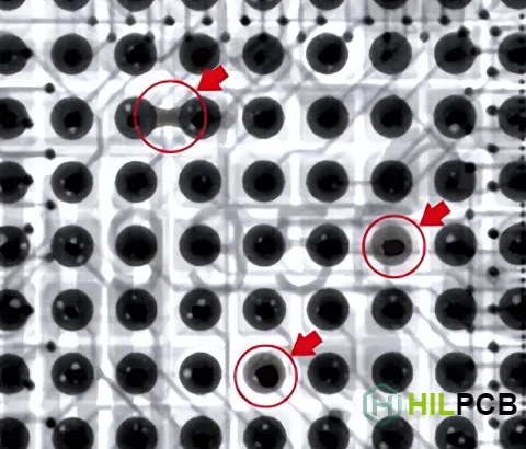
Open Connections and Non-Wetting
Open connections represent complete failure of solder joint formation. No electrical connection exists between component ball and PCB pad. Opens cause immediate functional failure but may affect only specific device functions depending on which connections fail.
Open defects result from various root causes requiring systematic investigation to identify and correct.
Open Connection Mechanisms
- Insufficient Solder: Paste volume inadequate to form joint; stencil life issues, clogged apertures, or printing parameters.
- Solder Ball Missing: Component shipped with missing ball or ball lost during handling; incoming inspection detects missing balls.
- Non-Wetting: Solder fails to wet pad surface due to oxidation, contamination, or inadequate flux activity; surface finish condition critical.
- Tombstoning: Primarily affects passive components but possible with small BGAs; uneven heating causes component lifting.
- Pad Contamination: Organic contamination, fingerprints, or process residues prevent solder wetting; cleaning procedures must be adequate.
- Insufficient Temperature: Peak temperature too low for complete solder melting and wetting; thermal profile verification required.
Prevention Approaches
- Paste Volume Control: Stencil design and printer setup ensure consistent paste volume; SPI verification confirms adequate deposition.
- Surface Finish Quality: Appropriate PCB surface finish selected and properly maintained; ENIG provides consistent solderability; storage conditions prevent degradation.
- Component Storage: Moisture control for MSL-sensitive components; oxidation prevention through proper packaging and handling.
- Profile Validation: Thermocouple profiling confirms all board areas reach adequate temperature; cold spots identified and corrected.
- Flux Activity: Paste flux formulation appropriate for surface conditions; no-clean fluxes may require better surface preparation.
Head-in-Pillow Defects
Head-in-pillow (HiP) defects represent partial connections where the component ball and solder paste partially melt but fail to fully coalesce. The joint appears connected but forms a weak mechanical connection prone to separation. HiP defects are particularly insidious because they may pass electrical test but fail in service.
Detection challenges make HiP defects among the most problematic BGA issues, requiring specific inspection techniques and process controls for prevention.
HiP Formation Mechanism
- Warpage Separation: Component or board warpage during reflow separates ball from paste during liquid phase; surfaces oxidize before rejoining.
- Oxide Formation: Surface oxides prevent coalescence even when ball and paste are both molten; flux insufficient to reduce oxides once formed.
- Timing Mismatch: Ball and paste melt at different times due to thermal gradients; earlier-melting material oxidizes before later material melts.
- Insufficient Flux: Flux consumed or volatilized before coalescence required; extended reflow profiles exhaust flux activity.
HiP Prevention Methods
- Warpage Reduction: Component specification for maximum warpage; PCB design and fabrication controls minimize board warpage.
- Reflow Atmosphere: Nitrogen atmosphere reduces oxidation during reflow; particularly effective for HiP prevention.
- Profile Optimization: Shorter time above liquidus reduces oxide formation opportunity; faster ramp rates may help but risk other defects.
- Flux Selection: Active flux formulations resist oxidation longer; trade-off with residue considerations for no-clean processes.
- Package-Specific Solutions: Problematic packages identified through qualification; vendor engagement for component-level improvements.
HiP Detection
- 3D X-Ray: Computed tomography reliably detects HiP by revealing the characteristic partial connection; 2D imaging often misses HiP defects.
- Dye Penetrant: Destructive technique reveals HiP through dye penetration into separation; used for process qualification.
- Electrical Test Limitations: HiP connections may pass continuity testing; resistance measurement may detect some but not all HiP conditions.
Solder Joint Voiding
Voiding occurs when gas bubbles remain trapped within solidified solder joints. Moderate voiding is normal and acceptable within defined limits, but excessive voiding degrades thermal conductivity and mechanical strength. Void location affects impact severity, with interface voids more concerning than bulk voids.
Voiding control requires understanding of formation mechanisms and process factors that influence void size and quantity.
Void Formation Mechanisms
- Flux Outgassing: Volatile flux components evaporating during reflow create bubbles; timing relative to solder solidification determines entrapment.
- Pad Contamination: Organic contamination volatilizes during reflow; residues from previous processes particularly problematic.
- Via-in-Pad: Improperly filled vias allow solder wicking and gas entrapment; proper via filling essential for void control.
- Solder Paste Chemistry: Paste formulation affects volatile content and outgassing timing; paste selection impacts void levels.
- Surface Finish: Certain surface finishes prone to higher voiding; ENIG generally produces lower voiding than some alternatives.
- Reflow Profile: Time at temperature affects outgassing completion; insufficient time prevents complete volatilization; excessive time may cause other issues.
Void Assessment
- X-Ray Quantification: BGA X-ray inspection enables void percentage measurement; automated image analysis provides consistent measurement.
- IPC-7095 Guidelines: Industry standard provides void acceptance criteria; Class 2 permits up to 25%; Class 3 restricts to 9-25% depending on void type.
- Location Assessment: Interface voids (at ball/pad boundary) more concerning than bulk voids; location affects acceptance decisions.
- Customer Specifications: Some applications impose stricter limits than IPC standards; aerospace and medical often require lower void levels.
Void Reduction Strategies
- Paste Selection: Low-void paste formulations available; trade-offs with other paste characteristics require evaluation.
- Profile Optimization: Extended soak time allows volatile escape before liquidus; faster ramp through liquidus reduces bubble entrapment opportunity.
- Vacuum Reflow: Specialty reflow equipment reduces atmosphere pressure during soldering; dramatically reduces voiding but adds cost.
- Via Treatment: Proper via filling per design rules; via-in-pad designs require appropriate fill and cap processes.
Component and Board Warpage Effects
Warpage during reflow creates non-uniform standoff heights across the BGA array. Corners and centers may lift away from or press toward the board depending on warpage direction. Warpage causes opens, bridges, or HiP defects depending on severity and direction.
Both component packages and PCBs contribute to warpage during thermal excursions. Combined effects determine actual standoff variation.
Warpage Sources
- Package Construction: Laminate substrate, die attach, and mold compound CTE mismatches cause temperature-dependent warpage; package design determines severity.
- PCB Construction: Asymmetric layer stackup, copper distribution, or material selection causes board warpage; design review identifies high-risk configurations.
- Thermal Gradients: Uneven heating during reflow causes temporary warpage; board support and reflow uniformity affect gradient magnitude.
- Residual Stress: Post-reflow warpage from stress relief; may differ from warpage during liquid phase when defects form.
Warpage Effects by Location
- Corner Opens: "Smiling" warpage lifts corners away from board; insufficient solder contact at corners creates opens.
- Center Opens: "Frowning" warpage lifts center; center balls fail to contact paste adequately.
- Combined Effects: Component and board warpage may add or partially cancel; worst case occurs when both warp in same direction.
- Dynamic Behavior: Warpage changes throughout reflow profile; maximum warpage may occur during temperature transitions.
Warpage Mitigation
- Component Specification: Maximum warpage specification in component procurement; problematic suppliers identified and replaced.
- Board Design Rules: Symmetric stackup, balanced copper, appropriate stiffness for board size; DFM review includes warpage assessment.
- Reflow Profile: Slower heating rates reduce thermal gradients; uniform heating minimizes temporary warpage.
- Board Support: Appropriate fixtures support large boards during reflow; prevents gravity-induced deflection.
Defect Prevention Strategies
Effective defect prevention combines proper design, capable processes, and systematic monitoring. Prevention costs far less than detection and rework, making investment in process capability highly economical.
Integrated prevention strategies address the interconnected causes of multiple defect types simultaneously.
Design Phase Prevention
- DFM Review: Manufacturing engineering review of designs before release identifies high-risk features; pad design, spacing, via strategy assessed.
- Package Selection: Components specified for acceptable warpage; MSL rating appropriate for assembly process; proven packages preferred.
- Thermal Simulation: Reflow simulation identifies thermal challenges before physical boards exist; enables design modification for manufacturability.
- Testability Design: Design for adequate electrical test coverage; in-circuit test access where feasible; boundary scan integration.
Process Phase Prevention
- Equipment Capability: Placement machines, reflow ovens, and inspection equipment matched to product requirements; capability studies verify performance.
- Process Validation: Qualification runs verify process capability before production; statistical analysis confirms defect rates meet targets.
- Operator Training: Trained personnel understand critical parameters and recognize abnormal conditions; certification programs ensure competency.
- Material Control: Solder paste, components, and boards stored and handled per requirements; shelf life and MSL managed appropriately.
Monitoring and Feedback
- Statistical Process Control: Key parameters monitored and controlled; out-of-control conditions trigger investigation before defects occur.
- Inspection Data Analysis: Defect data analyzed for patterns indicating root causes; trend analysis identifies emerging issues.
- Corrective Action: Systematic problem solving addresses identified issues; verification confirms effectiveness of corrections.
- Continuous Improvement: Regular process optimization reduces defect rates over time; benchmark against industry best practices.
HILPCB Defect Prevention Capabilities
HILPCB applies comprehensive defect prevention strategies throughout our SMT assembly processes. Our approach combines design support, process control, and thorough inspection to deliver reliable BGA assemblies.
Prevention Through Expertise
Design for Manufacturing Review
Our engineering team reviews BGA designs before production, identifying features that increase defect risk. Recommendations for pad design, via strategy, and component selection prevent issues before they occur.
Process Capability
Investment in modern equipment provides the placement accuracy, reflow control, and inspection capability required for demanding BGA assemblies. Regular capability studies verify continued performance.
Statistical Process Control
Key process parameters are monitored using SPC techniques. Control charts identify drift before defects occur, enabling proactive adjustment rather than reactive rework.
Comprehensive Inspection
- Solder paste inspection verifies deposition before placement
- X-ray inspection detects hidden defects after reflow
- Automated inspection programs ensure consistent evaluation
Rework Capability
When defects occur despite prevention efforts, our BGA rework capabilities enable correction. Quick turnaround on rework minimizes schedule impact.
Continuous Improvement
Defect data analysis identifies improvement opportunities. Process refinements reduce defect rates over time, benefiting all customers through lower costs and higher quality.
Contact HILPCB for BGA assembly services with the process control and inspection capabilities your quality requirements demand.