
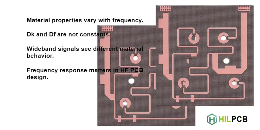
PCB material properties vary with frequency—dielectric constant decreases, loss tangent may change, and propagation characteristics shift across the spectrum. For wideband applications spanning multiple octaves or requiring consistent performance from DC to daylight, understanding material frequency response is essential for successful design.
This guide provides comprehensive knowledge of frequency-dependent material behavior and its implications for HF PCB material performance in wideband applications.
HILPCB offers materials characterized across wide frequency ranges, with engineering support for selecting materials that meet your wideband requirements for RF and microwave circuit fabrication.
Frequency Dependence of Dielectric Constant
Dielectric constant (Dk) varies with frequency due to the time required for molecular polarization to respond to changing electric fields. This variation affects impedance, velocity, and wavelength across the operating bandwidth.
At HILPCB, we provide frequency-characterized material data to support accurate wideband design.
Polarization Mechanisms
Different polarization mechanisms dominate at different frequencies:
- Electronic polarization: Fastest, active to optical frequencies
- Ionic polarization: Slower, contributes below ~THz
- Dipolar polarization: Much slower, contributes to MHz-GHz
- Interfacial polarization: Slowest, low-frequency effect
As frequency increases, slower mechanisms can't follow the field, and Dk decreases.
Typical Dk Frequency Behavior
Most PCB materials show decreasing Dk with increasing frequency:
| Material | Dk @ 1 MHz | Dk @ 1 GHz | Dk @ 10 GHz |
|---|---|---|---|
| Standard FR-4 | 4.7 | 4.4 | 4.0 |
| Low-loss FR-4 | 4.0 | 3.8 | 3.6 |
| Rogers RO4350B | 3.66 | 3.52 | 3.48 |
| PTFE | 2.20 | 2.18 | 2.17 |
PTFE and ceramic-filled materials show the most stable Dk across frequency.
Impedance Variation
Frequency-dependent Dk causes frequency-dependent impedance:
- Higher frequency sees lower Dk
- Lower Dk means higher impedance for same geometry
- Wideband signals experience different impedance at different frequencies
For 10% Dk variation: ~5% impedance variation across bandwidth.
Design Implications
For wideband designs:
- Use materials with stable Dk (PTFE, ceramic-filled)
- Characterize material at center frequency
- Account for impedance variation in margin analysis
- Consider frequency-dependent matching
Frequency Dependence of Loss
Loss tangent (Df) also varies with frequency, though the pattern differs by material type. Understanding this variation enables accurate loss prediction across bandwidth.
For wideband low-loss requirements, HILPCB offers fluoropolymer laminates with stable loss characteristics.
Loss Mechanisms by Frequency
- Conduction loss: Present at all frequencies, DC component
- Polarization loss: Peaks at relaxation frequencies
- Resonance loss: Material-specific resonances
Material-Specific Behavior
Different materials show different Df trends:
- FR-4: Df generally increases with frequency (relaxation effects)
- PTFE: Df relatively flat or slightly decreasing
- Ceramic-filled: Generally stable across frequency
Dk Stability Across Frequency
Total Loss Frequency Dependence
Total transmission line loss combines:
- Conductor loss: Increases with √f
- Dielectric loss: Increases approximately linearly with f
At low frequencies, conductor loss dominates. At high frequencies, dielectric loss dominates. Crossover frequency depends on material and geometry.
Wideband Loss Estimation
For accurate wideband loss prediction:
- Use frequency-specific Df values
- Calculate loss at multiple frequencies
- Consider both conductor and dielectric contributions
- Account for dispersion in pulse response
Dispersion and Signal Distortion
When propagation velocity varies with frequency (due to Dk frequency dependence), signals disperse—different frequency components travel at different speeds, causing pulse spreading and distortion.
Understanding dispersion: Dielectric Properties of HF PCB
Dispersion Mechanism
Phase velocity in transmission line:
v_p = c / √Dk_eff
If Dk varies with frequency, v_p varies, causing:
- Different frequency components arrive at different times
- Sharp pulse edges spread
- Pre-shoot and post-shoot on waveforms
- Increased inter-symbol interference
Group Delay Variation
Group delay measures how fast signal envelope propagates:
τ_g = -dφ/dω
Frequency-dependent Dk causes group delay variation across bandwidth. This variation indicates dispersion severity.
Impact on Digital Signals
Wideband digital signals contain many harmonics. Dispersion:
- Rounds pulse edges
- Reduces eye opening
- Increases jitter
- Worsens ISI
Fast rise time signals are most affected.
Minimizing Dispersion
For minimum dispersion:
- Select materials with stable Dk (PTFE, ceramic)
- Use shorter traces (less time for spreading)
- Consider equalization to compensate
- Design for achievable rather than ideal rise times
Wideband Design Considerations
Practical approaches to designing circuits that operate across wide frequency ranges.
For wideband applications, HILPCB provides precision RF PCB manufacturing with characterized materials.
Material Selection Criteria
For wideband applications, prioritize:
- Dk stability across frequency (minimize dispersion)
- Low Df across entire bandwidth (minimize loss variation)
- Dk tolerance (consistent impedance)
- Temperature stability (consistent across operating range)
Impedance Matching Bandwidth
Wideband matching challenges:
- Component values are frequency-dependent
- Transmission line matching varies with Dk
- Lumped element matching has bandwidth limits
Strategies:
- Use distributed matching for wider bandwidth
- Account for Dk variation in matching network design
- Consider tapered transitions for very wideband
Transition Structures
Wideband transitions (connectors, vias) require careful design:
- Minimize discontinuity at all frequencies
- Via compensation may need to be frequency-weighted
- Connector launch optimization for bandwidth
Simulation Approach
For accurate wideband simulation:
- Use frequency-dependent material models
- Include skin effect conductor models
- Simulate across entire bandwidth of interest
- Verify with frequency-domain measurements
Material Characterization Methods
Accurate characterization provides the data needed for precise wideband design.
HILPCB works with characterized materials and can provide data sheets with frequency-dependent properties.
Resonant Methods
Split-post dielectric resonator:
- High accuracy at discrete frequencies
- Measures Dk and Df simultaneously
- Standard method (IPC-TM-650 2.5.5.13)
- Typical frequencies: 1-20 GHz
Cavity resonator:
- Very high accuracy
- Single frequency per cavity
- Reference method for material qualification
Transmission Line Methods
Microstrip or stripline test structures:
- Broadband measurement possible
- Requires accurate fixture calibration
- Extracts Dk and Df from S-parameters
- Practical for production verification
Full-Wave Extraction
From S-parameter measurements:
- Measure test structure with VNA
- De-embed fixture effects
- Extract material parameters using models
- Provides broadband Dk and Df curves
Data Sheet Interpretation
Material data sheets may specify:
- Dk at single frequency (often 10 GHz)
- Dk at multiple frequencies (better)
- Dk tolerance
- Df at single or multiple frequencies
For wideband design, request multi-frequency data or use published curves.
Material Options for Wideband Applications
Materials optimized for wideband performance.
HILPCB stocks wideband-suitable materials including Rogers high-frequency laminates.
PTFE-Based Materials
Best Dk stability for wideband:
- Rogers RT/duroid 5880: Dk 2.20, very stable
- Taconic TLY: Dk 2.2, excellent stability
- Arlon DiClad: Dk 2.5, good stability
Challenges: Special processing, higher cost
Ceramic-Filled Hydrocarbon
Good stability with easier processing:
- Rogers RO4350B: Dk 3.48, good stability
- Rogers RO4003C: Dk 3.55, similar performance
- Isola Astra: Dk 3.0, low-loss ceramic
FR-4 compatible processing, moderate cost.
Low-Loss FR-4 Variants
For cost-sensitive wideband (up to ~10 GHz):
- Panasonic Megtron 6: Good stability
- Isola I-Tera MT40: Moderate stability
- Various vendor options
Standard processing, lowest HF material cost.
Related Material Performance Topics
- High Frequency PCB Material Performance: Complete material selection guide
- Dielectric Properties of HF PCB: Dk and Df fundamentals
- Material Loss Factor in HF PCB: Loss mechanisms
- Thermal Stability in High Frequency PCB: Temperature effects
- Moisture Effects on HF PCB Material: Humidity impacts
HILPCB Wideband Material Services
HILPCB delivers materials for wideband high frequency applications:
Characterized Materials: Materials with documented frequency response data for accurate wideband design.
Material Selection Support: Engineering consultation for selecting materials meeting your bandwidth and stability requirements.
Process Control: Consistent manufacturing that preserves characterized material properties.
Verification: S-parameter testing available to verify wideband performance meets requirements.
From prototype wideband circuits through production volumes, HILPCB provides frequency-stable materials for demanding wideband applications.
Contact HILPCB for wideband material consultation and manufacturing quotation.