
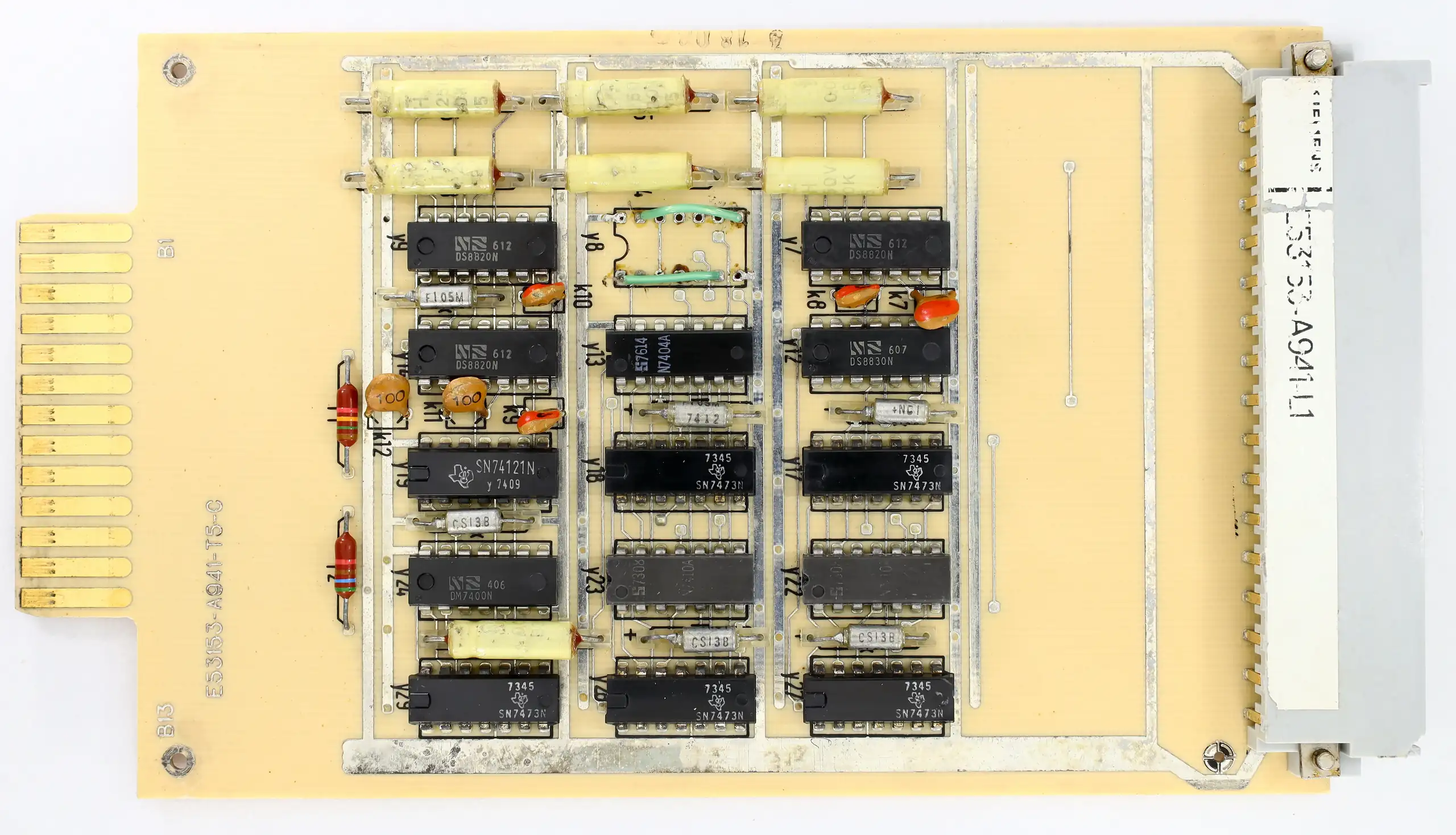
An industrial fieldbus interface PCB is a board that carries the physical communication interface between industrial controllers, gateways, sensors, drives, I/O modules and factory networks. The PCB does not certify a protocol by itself; it provides the port-level layout, isolation boundary, surge protection, EMC filtering, connector strategy and manufacturing quality needed before the complete device can be validated.
This guide is written for hardware teams releasing RS-485, CANopen, EtherCAT, PROFINET, Modbus, industrial gateway or PLC interface boards. It focuses on board-level decisions that affect manufacturability, field reliability and RFQ clarity without turning protocol names into unsupported conformance claims.
Key Takeaways
- Use protocol names as design context, not as proof of conformance. An EtherCAT or PROFINET interface chip does not make the finished device certified.
- Review the communication port as a subsystem: connector, shield/chassis transition, surge path, isolation barrier, common-mode control, routing into the PHY or transceiver and test access.
- Industrial fieldbus boards often fail at the boundary between field wiring and logic ground, not inside the digital protocol stack.
- Isolation, creepage, clearance, surge and EMC requirements must be set from the target device, installation environment and certification plan, not from a generic blog table.
- A useful RFQ package should include the protocol interface type, connector plan, isolation targets, EMC test intent, stackup needs, component constraints and assembled-board test expectations.
In This Guide
- What an industrial fieldbus interface PCB review approves
- Protocol names: RS-485, CANopen, EtherCAT and PROFINET
- Fieldbus interface PCB architecture
- Isolation, creepage and surge protection
- EMC and signal-integrity layout rules
- Connector, cable and shielding decisions
- Power integrity and grounding
- Common failure modes before release
- Manufacturing and test controls
- Cost drivers in industrial fieldbus boards
- RFQ checklist for fieldbus interface PCB projects
- Why choose HILPCB for industrial interface boards
- Reference standards and specifications
- FAQ
What an industrial fieldbus interface PCB review approves
A fieldbus interface PCB review approves whether the board architecture is ready for manufacturing review and first-build validation. It does not approve the final device for field use, protocol conformance or machinery safety.
That distinction matters because fieldbus projects often arrive with protocol labels that sound more complete than the hardware really is. A drawing may say RS-485, CANopen, EtherCAT, PROFINET or industrial gateway, but the PCB release package still has to answer board-level questions:
- Where does the field cable enter the board?
- Which parts are on the field side and which parts are on the logic side?
- Is galvanic isolation required between the bus and system ground?
- What surge, ESD and EFT protection is expected at the port?
- How are cable shields or chassis connections handled?
- Can the port zone be inspected, probed and functionally tested after assembly?
- Which claims must remain device-level or certification-lab-level instead of PCB-level?
For a release review, a strong fieldbus PCB description should therefore say less about the protocol stack and more about the physical interface story. The board must have a visible port boundary, a controlled return path, a coherent protection path and a realistic manufacturing handoff.
Project Boundary
HILPCB can manufacture and assemble industrial fieldbus interface PCBs according to the supplied design data, stackup requirements, impedance notes, isolation keepouts, material requirements and test instructions. Final protocol certification, system EMC results, functional safety claims, machine-level compliance and field interoperability must be validated at the device or system level by the product owner and, where required, by the relevant test body.
Protocol names: RS-485, CANopen, EtherCAT and PROFINET
A protocol name is useful when it tells the PCB manufacturer what kind of physical interface and layout discipline the board needs. It becomes risky when it is used as a certification claim.
| Interface name | What it usually means for the PCB | What it does not prove by itself | Typical board review focus |
|---|---|---|---|
| RS-485 / TIA-485 | Differential serial bus interface, often used for Modbus RTU and other industrial links | Protocol behavior, bus timing, site wiring quality or EMC pass result | Transceiver placement, termination, biasing, surge protection, isolation and connector layout |
| CAN / CANopen | CAN physical layer with CANopen application/profile context | CANopen device certification, interoperability or correct object dictionary behavior | CAN transceiver routing, split termination, common-mode control, isolation and ESD protection |
| EtherCAT | Industrial Ethernet device interface using EtherCAT technology | EtherCAT conformance or accepted vendor implementation | PHY layout, magnetics, connector/shield transition, reference-clock integrity and differential-pair control |
| PROFINET | Industrial Ethernet interface for automation systems | PI certification, conformance class, interoperability or network performance | Ethernet PHY layout, magnetics, RJ45/M12 connector zone, EMI filtering and EMC test access |
| Industrial gateway | Multi-protocol or protocol-conversion board | Successful translation between protocols or field-device compatibility | Port separation, isolation strategy, power domains, CPU/SoM integration, thermal and test planning |
For search intent, this is important: a buyer searching for “EtherCAT PCB” or “PROFINET PCB” usually wants a hardware partner who understands industrial Ethernet layout and manufacturing constraints. They do not need an unsupported promise that the bare PCB is certified. Device conformance is a separate program involving the full hardware, firmware, protocol stack and test procedure.
Fieldbus interface PCB architecture
A robust fieldbus interface board is easiest to review when the port area is treated as a defined subsystem instead of a few scattered parts near the connector.
A typical architecture contains five zones:
- Field wiring zone: terminal block, RJ45, M12, D-sub, spring clamp, pluggable header or other industrial connector.
- Protection zone: TVS diodes, common-mode choke, series resistors, GDT/MOV where appropriate, ESD structures and cable-shield transition.
- Isolation zone: digital isolator, isolated transceiver, transformer magnetics, isolated DC/DC module or keepout barrier.
- PHY/transceiver zone: RS-485, CAN, Ethernet PHY, industrial Ethernet controller or gateway interface chip.
- Logic and system zone: MCU, FPGA, SoM, CPU, memory, power regulation, diagnostics and host interface.
The release review should make those zones visible in the layout. When a surge device sits far from the connector, when a shield path crosses sensitive logic, or when isolation keepouts are broken by copper pours, silkscreen, mounting hardware or test pads, the issue is not just electrical. It becomes a manufacturing and reliability risk.
Fieldbus architecture review table
| Board area | What to check | Why it matters | Manufacturing evidence to include |
|---|---|---|---|
| Connector edge | Entry direction, enclosure fit, mating height and cable strain path | Connector geometry can force routing compromises and assembly access issues | Mechanical drawing, connector datasheets, keepout notes |
| Protection zone | Short, low-inductance path from connector pins to protection parts | Long protection traces can make TVS or surge parts less effective | Placement screenshot, BOM notes, copper path review |
| Isolation barrier | Keepout shape, slotting, copper clearance and component orientation | Isolation only works if the physical barrier is maintained through PCB fabrication and assembly | Isolation keepout layer, fabrication notes, assembly constraints |
| Signal routing | Differential pair control, symmetry, stubs, return path and layer transitions | Poor routing can create reflections, common-mode noise and EMI problems | Stackup, impedance table, length/skew notes where needed |
| Test access | Probe points, boundary-scan plan, loopback options or fixture pads | Interface boards are hard to debug after connectors and shielding are mounted | Test-pad drawing, functional test requirements |
Isolation, creepage and surge protection
Industrial fieldbus boards often connect equipment that sits far apart, shares noisy power systems or runs next to motor drives and solenoids. The PCB should therefore be reviewed against a realistic field environment, not only against lab-bench communication.
Galvanic isolation
Isolation separates field-side signal energy from logic-side ground. It may be implemented with isolated RS-485/CAN transceivers, digital isolators plus separate PHYs, Ethernet magnetics or isolated DC/DC power domains.
At PCB level, isolation review is not only about the component rating. It also includes:
- uninterrupted isolation keepout between field and logic domains
- no copper pour, test pad, via stitching or silkscreen bridge across the isolation barrier
- adequate spacing around optocouplers, digital isolators, transformers and isolated power modules
- slotting strategy where required by the project’s insulation target
- controlled Y-capacitor or chassis path if common-mode noise needs a defined return
Exact creepage and clearance values should come from the applicable insulation standard, working voltage, pollution degree, overvoltage category, material group and certification plan. A blog should not replace that engineering calculation.
Surge, ESD and EFT protection
A protection circuit is only as good as its layout. TVS diodes, common-mode chokes, series elements and surge components must be close enough to the connector to intercept energy before it travels through the board.
| Protection concern | Board-level design control | Common mistake | Release-review question |
|---|---|---|---|
| ESD at connector | Place ESD/TVS parts close to entry pins with short return to chassis or defined reference | Protection part placed near transceiver instead of connector | Does the transient current have a short path that avoids sensitive circuitry? |
| EFT/burst coupling | Use filtering and controlled cable-entry routing | Long parallel runs from connector to logic side | Are noisy entry traces kept away from high-impedance or clock circuits? |
| Surge event | Use project-specified TVS, GDT, MOV or coordinated protection scheme | Component selected by voltage rating only, without layout review | Is the protection part coordinated with the expected transient and grounding path? |
| Ground potential difference | Use galvanic isolation or robust common-mode design where needed | Non-isolated bus tied directly to logic ground across long plant wiring | Has the installation environment been considered? |
| Cable shield current | Define chassis/shield connection strategy | Shield connected randomly to digital ground through thin copper | Is shield current routed away from logic return and signal reference? |
EMC and signal-integrity layout rules
Industrial interface boards need both communication integrity and electromagnetic robustness. Those goals can conflict. For example, aggressive filtering can protect the port but distort fast edges; a continuous ground plane can improve signal return but must not violate the isolation strategy.
RS-485 and CAN layout
RS-485 and CAN are differential interfaces, but differential signaling is not a license to route carelessly. The board should preserve pair symmetry, avoid unnecessary stubs and give the return path a controlled route.
Practical checks include:
- keep A/B or CANH/CANL traces close and symmetric from connector to transceiver
- keep termination and biasing components close to the bus entry or transceiver according to the circuit topology
- avoid routing the bus pair through split planes unless the return path is intentionally controlled
- keep isolated and non-isolated grounds clearly separated
- keep high dv/dt switching nodes away from the bus pair and protection zone
- provide test access for bus state, termination and loopback where the test plan requires it
EtherCAT and PROFINET layout
Industrial Ethernet ports add PHY, magnetics and connector constraints. The board does not become compliant because the PHY is present; the port still needs a controlled layout.
Review items include:
- differential-pair impedance control according to stackup and PHY requirements
- short, symmetric routing between PHY, magnetics and connector
- clock source placement and low-noise reference routing
- magnetics orientation and isolation boundary control
- connector shield/chassis transition strategy
- EMI filter placement that does not break the intended return path
Mixed protocol gateway boards
Gateway boards often combine RS-485, CAN, Ethernet, USB, cellular, Wi-Fi, I/O and power conversion on one PCB. In these boards, the most common layout risk is not a single protocol trace. It is uncontrolled coupling between several interface zones.
For multi-port industrial gateways, consider reviewing each port as its own threat model: cable length, external power, shield behavior, isolation need, ESD exposure, service access and thermal load.
Connector, cable and shielding decisions
Connector choice affects electrical design, mechanical packaging and assembly inspection. It should not be decided after the layout is mostly complete.
| Connector / interface style | Where it is commonly used | PCB design impact | RFQ notes to provide |
|---|---|---|---|
| Pluggable terminal block | RS-485, CAN, power and I/O modules | Large edge keepout, screw access, strain relief and field wiring direction | Pitch, orientation, current rating, mating part, enclosure constraints |
| RJ45 | Ethernet, PROFINET, EtherCAT development or cabinet devices | Magnetics/shield routing, connector height and EMI control | Shielded/unshielded, integrated magnetics or external magnetics, LED needs |
| M12 | Industrial Ethernet and rugged field devices | Circular connector mechanics, panel mount and cable strain requirements | Coding type, pinout, panel relationship, environmental requirements |
| D-sub | Legacy industrial serial, test equipment and gateway products | Large footprint, mounting posts and shell grounding | Shield connection, screw lock details, mating cable requirement |
| Board-to-board / mezzanine | Modular PLC or gateway architecture | Stack height, impedance continuity and assembly sequence | Mating connector, tolerance stack, service replacement needs |
Cable shield handling deserves early review. A shield path may connect to chassis directly, through capacitive coupling, through RC networks or according to the customer’s system design. The PCB should not silently force shield current into digital ground unless that is the intended system architecture.
Power integrity and grounding
Fieldbus boards often mix noisy power domains with sensitive communication interfaces. The release package should show how power enters the board, how isolated power is generated and how return currents are kept out of the port boundary.
Key controls include:
- keep switching regulators away from PHY/transceiver inputs and crystal/clock regions
- give isolated DC/DC modules a defined keepout and return strategy
- place decoupling capacitors close to transceivers, PHYs and isolators
- separate chassis, field-side ground, isolated ground and logic ground intentionally
- avoid thin, long return paths for protection currents
- route hot-loop switching currents compactly and away from bus traces
For higher-layer-count gateway boards, a High-Speed PCB stackup review is often more useful than treating the design as a generic industrial control board. For ports with tight edge rates, RF-like connector transitions or mixed Ethernet and wireless sections, High-Frequency PCB review may also be relevant.
Common failure modes before release
The most useful fieldbus PCB review is the one that finds failures before the first pilot build.
| Failure mode | Likely board-level cause | Field symptom | Prevention before release |
|---|---|---|---|
| Transceiver destroyed after cable plug-in | ESD/surge parts too far from connector or weak return path | Port dead after installation or service handling | Move protection to entry point; define chassis/return path |
| Intermittent communication on long cable | Bad termination, stubs, poor differential routing or common-mode shift | Random CRC errors, retries or dropouts | Review bus topology, pair routing, termination and isolation need |
| EMC test failure | Cable shield current enters logic ground; filter placement ineffective | Radiated or conducted emissions/immunity issue | Review shield/chassis transition and common-mode choke placement |
| Isolation barrier compromised | Copper pour, via, silkscreen, test point or component violates keepout | Safety or insulation review failure | Add dedicated isolation keepout layer and fabrication note |
| Gateway resets during motor start | Surge or EFT couples into power or reset circuit | Device reboot when nearby drive or relay switches | Add port protection, filtering and power-domain review |
| Ethernet link unstable | PHY-magnetics-connector routing too long or asymmetric | Link drop, negotiation problem or packet loss | Review differential-pair impedance, pair length and magnetics placement |
| Assembly access blocked | Tall connector or shield covers test pads | Low production test yield or manual rework | Move test pads and define fixture access before layout freeze |
| Wrong connector orientation | Mechanical drawing not aligned with enclosure or cable entry | Cable cannot mate after installation | Include 3D model and enclosure-facing drawing in RFQ |
Manufacturing and test controls
Industrial fieldbus interface boards usually need stronger manufacturing discipline than simple controller boards because the connector boundary, isolation barrier and protection components are all sensitive to layout and assembly variation.
Bare-board controls
- impedance control for Ethernet, high-speed host links or any customer-specified controlled traces
- laminate and stackup review for isolation slots, layer symmetry and copper balance
- solder mask clearance review around fine-pitch PHYs and interface ICs
- routing inspection around isolation keepouts and slotted barriers
- electrical test according to supplied netlist
- dimensional checks for connector-edge and enclosure-critical features
PCBA controls
- AOI for polarity-sensitive protection parts, isolators, PHYs and connectors
- X-ray where hidden solder joints or critical packages require it
- connector coplanarity and alignment checks
- functional test or loopback test where the customer supplies firmware and fixture requirements
- Hi-pot or insulation-resistance testing only when the project specification defines method, voltage, duration and pass criteria
- conformal coating, selective coating or potting control when the installation environment requires it
Do not write “tested to IEC 61000” or “certified interface board” unless the full test program, lab report and product scope support that statement. For PCB content, it is safer to say the board is designed to support the customer’s EMC or conformance test plan.
Cost drivers in industrial fieldbus boards
Cost is not only about board size. In fieldbus interface PCBs, the expensive choices often come from isolation, protection, connector mechanics and testability.
| Cost driver | Why it increases cost | How to control it without weakening reliability |
|---|---|---|
| Higher layer count | Needed for dense routing, clean returns, Ethernet pairs or gateway CPU sections | Use stackup review early; avoid adding layers after routing congestion appears |
| Controlled impedance | Required for Ethernet, high-speed host interfaces and some gateway designs | Provide target impedance, tolerance and material preference in RFQ |
| Isolation slots / keepouts | Reduce routing area and add fabrication constraints | Define isolation zones before component placement |
| Industrial connectors | Large footprints, mounting hardware and manual assembly requirements | Freeze connector model and mating direction before PCB layout |
| Surge and EMC protection | Adds BOM cost and placement area | Select protection based on environment and test plan, not generic overdesign |
| Conformal coating or potting | Adds process steps and inspection limits | Use selective protection only where the application needs it |
| Functional test fixture | Needed for assembled boards and multi-port gateways | Include test points and firmware/fixture plan before production release |
RFQ checklist for fieldbus interface PCB projects
A complete RFQ package reduces redesign risk and helps the manufacturer review the right parts of the board.
Design files
- Gerber, ODB++ or IPC-2581 package
- drill files, netlist and fabrication drawing
- assembly drawing, centroid file and BOM for PCBA
- stackup target and controlled-impedance requirements
- 3D model or mechanical outline if connector alignment is critical
Interface and protocol context
- fieldbus or industrial Ethernet interface type: RS-485, CAN, CANopen, EtherCAT, PROFINET, Modbus, gateway or other
- number of ports and whether they are isolated
- expected connector type, orientation and mating part
- termination, biasing and shield strategy if already defined
- PHY/transceiver part numbers and any vendor layout requirements
Protection and environment
- ESD, EFT, surge or EMC test intent if known
- operating voltage, external cable length and installation environment
- isolation rating target, creepage/clearance requirements and slotting notes
- conformal coating, potting or corrosion-resistance requirements
- operating temperature and humidity range
Manufacturing and testing
- prototype quantity and mass-production forecast
- IPC class requirement if specified
- AOI, X-ray, functional test, programming or serialization needs
- loopback test, boundary-scan, firmware or fixture requirements
- labeling, traceability and packaging requirements
Why choose HILPCB for industrial interface boards
HILPCB supports industrial communication projects that require more than a simple control-board build. For fieldbus and industrial Ethernet applications, our engineering review can focus on stackup, impedance, connector manufacturability, isolation-zone preservation, assembly process and test-access planning.
Relevant manufacturing paths include:
- High-Speed PCB for controlled impedance, Ethernet PHY routing, gateway CPU interfaces and dense digital sections.
- High-Frequency PCB for projects where edge-rate control, connector transitions or mixed RF/industrial sections need tighter material and layout review.
- HDI PCB for compact gateway boards, dense controllers and modules with fine-pitch components.
- Turnkey Assembly for projects that require component sourcing, SMT assembly, connector assembly, inspection and functional-test coordination.
Send your Gerber package, stackup target, BOM, connector drawings and interface requirements through the Quote page for DFM and manufacturing review.
Reference standards and specifications
These references are listed for engineering context only. They should not be used to imply that a bare PCB is certified or that a finished product has passed conformance testing.
- IEC 61158 — Industrial communication networks, fieldbus specifications
- IEC 61784 — Industrial communication networks, profiles
- TIA-485 / ANSI/TIA/EIA-485-A — Electrical characteristics for balanced multipoint serial interfaces
- IEC 61000-4-2 — ESD immunity test methods
- IEC 61000-4-4 — Electrical fast transient / burst immunity test methods
- IEC 61000-4-5 — Surge immunity test methods
- CISPR 11 — Industrial, scientific and medical equipment radio-frequency disturbance characteristics
- IEC 61131 — Programmable controllers
- IEC 62061 — Safety of machinery, functional safety of safety-related control systems
- ISO 13849 — Safety-related parts of control systems
- CiA 301 — CANopen application layer and communication profile
- EtherCAT Technology Group conformance documentation
- PROFIBUS & PROFINET International certification documentation
FAQ
Can a PCB itself be PROFINET or EtherCAT certified?
No. A bare PCB or assembled interface board does not become certified just because it uses a PROFINET or EtherCAT PHY, controller or connector. Certification and conformance programs apply to the complete device implementation, including hardware, firmware, stack behavior, device description files and test procedure.
Is RS-485 the same thing as Modbus?
No. RS-485, more precisely TIA-485, defines the electrical characteristics of a balanced multipoint interface. Modbus RTU is a communication protocol that is often carried over RS-485 wiring. The PCB review should therefore cover the physical RS-485 interface while the product owner validates protocol behavior.
When should an industrial fieldbus interface use galvanic isolation?
Isolation should be considered when the board connects to long cables, different ground potentials, outdoor wiring, high-noise machines, motor drives or service environments where surge and common-mode stress are likely. The exact isolation rating and spacing must come from the product’s safety and EMC plan.
What is the most common layout mistake on fieldbus ports?
A common mistake is placing surge or ESD protection too far from the connector, forcing transient current to travel through sensitive board areas before it reaches the protection device. Protection parts should be reviewed together with the return path, chassis connection and isolation boundary.
Do Ethernet-based fieldbus boards need controlled impedance?
Yes, industrial Ethernet ports such as EtherCAT and PROFINET typically require controlled differential-pair routing between PHY, magnetics and connector. The target impedance and tolerance should be defined in the stackup and verified with the PCB manufacturer.
What should I send for a fieldbus interface PCB quote?
Send Gerber or ODB++ files, BOM, assembly drawings, stackup requirements, interface type, connector drawings, isolation targets, protection requirements, operating environment, coating or potting needs and any functional-test instructions. For PCBA projects, include firmware or loopback-test requirements if available.
Can HILPCB perform final protocol conformance testing?
HILPCB can support PCB manufacturing, assembly and board-level test planning according to your supplied requirements. Final protocol conformance, interoperability and certification testing should be performed by the product owner or the relevant official test body.
Next step
If your fieldbus interface board already has a schematic, connector plan and early layout, send the design package through the Quote page. HILPCB can review the manufacturing risks around port protection, isolation keepouts, controlled impedance, connector assembly and test access before the project moves into prototype or production.