
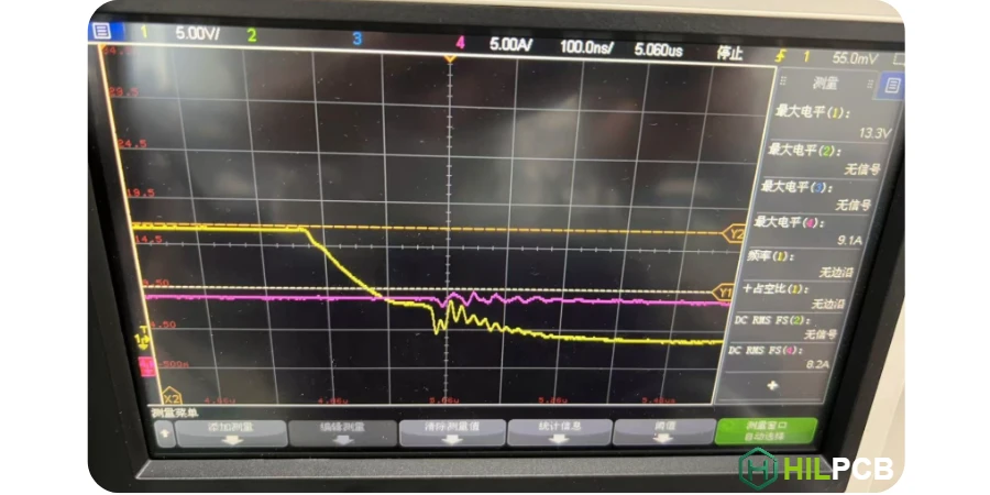
Signal distortion occurs when a waveform changes shape as it travels through a PCB—the signal arriving at the receiver differs from what the transmitter sent. At high frequencies, multiple distortion mechanisms combine to degrade signal quality, potentially causing data errors and system failures.
Understanding distortion sources and their remedies is essential for high frequency PCB signal integrity.
HILPCB manufactures high frequency PCBs with controlled impedance (±5% standard, ±3% critical) and low-loss materials that minimize distortion in demanding applications.
In This Guide
- What Is Signal Distortion
- Types of Signal Distortion
- Causes of Distortion in HF PCBs
- Measuring and Analyzing Distortion
- Design Strategies to Reduce Distortion
- Material and Manufacturing Considerations
- Real-World Applications
What Is Signal Distortion
Signal distortion is any unintended change in waveform shape between transmitter output and receiver input. In ideal conditions, a signal would travel through a PCB unchanged—but real PCBs introduce multiple impairments that alter the waveform.
Why Distortion Matters
Digital systems rely on distinguishing between logic high and low states. Distortion reduces the margin between these states, making the receiver's job harder. Severe distortion causes:
- Bit errors: Receiver misinterprets signal state
- Timing violations: Signal transitions occur at wrong times
- Reduced noise margin: Less tolerance for additional interference
- Failed compliance testing: Eye diagram doesn't meet specifications
The Frequency Connection
Distortion increases with frequency because:
- Higher frequencies experience more loss
- Faster edges contain more high-frequency content
- Timing margins shrink at higher data rates
- Multiple impairments compound
A signal that looks clean at 1 Gbps may be severely distorted at 10 Gbps on the same PCB—the physics don't change, but the requirements become more demanding.
Types of Signal Distortion
Understanding different distortion mechanisms helps identify appropriate solutions.
Amplitude Distortion
Signal amplitude changes as it propagates—typically decreasing due to losses. If high frequencies attenuate more than low frequencies (which they do), the waveform shape changes.
Effect: Reduced signal swing, slower transitions, decreased noise margin.
Related topic: Signal Attenuation in High Frequency PCB
Phase Distortion
Different frequency components experience different delays. Since complex waveforms contain multiple frequencies, phase distortion alters the relative timing of these components, changing waveform shape.
Effect: Edge timing shifts, duty cycle distortion, inter-symbol interference.
Related topic: Phase Delay in High Frequency PCB
Harmonic Distortion
Non-linear elements generate frequencies not present in the original signal. While less common in passive PCB structures, it can occur at connector interfaces or with certain via geometries at very high power levels.
Effect: Spurious frequency content, EMI issues.
Inter-Symbol Interference (ISI)
Perhaps the most important distortion mechanism in high-speed digital: energy from one bit period "bleeds" into adjacent bit periods. Previous bits affect the current bit's voltage level.
Effect: Eye closure, pattern-dependent jitter, increased bit error rate.
Distortion Impact on Eye Diagram
Causes of Distortion in HF PCBs
Multiple PCB characteristics contribute to signal distortion. Identifying dominant causes in your design guides mitigation efforts.
Frequency-Dependent Loss
Both conductor loss (skin effect) and dielectric loss increase with frequency. Since digital signals contain a spectrum of frequencies (fundamental plus harmonics), higher frequency components attenuate more than lower ones—changing the waveform shape.
Impact: Slower rise/fall times, reduced amplitude, ISI
Mitigation: Shorter traces, lower-loss materials, wider traces (reduces skin effect loss)
Impedance Discontinuities
Every impedance mismatch reflects a portion of signal energy. These reflections travel back and forth, adding to the original signal at various delays. The composite waveform shows ringing, overshoot, and undershoot.
Impact: Ringing, non-monotonic edges, false triggering
Mitigation: Consistent impedance design, proper termination, minimizing via transitions
Dispersion
In real materials, propagation velocity varies slightly with frequency (dielectric constant is frequency-dependent). Different frequency components arrive at different times, spreading the signal.
Impact: Edge spreading, increased rise time, ISI
Mitigation: Lower-dispersion materials, shorter traces
Via Discontinuities
Vias introduce both impedance discontinuity (via barrel impedance differs from trace) and stub resonance (unused via barrel creates resonant stub). At high frequencies, via stubs can severely attenuate specific frequencies.
Impact: Notches in frequency response, reflections, loss
Mitigation: Back-drilling, blind/buried vias, optimized via geometry
Crosstalk
Energy coupled from adjacent signals adds to the victim signal. This coupling is frequency-dependent and can significantly alter waveform shape, especially on long parallel runs.
Impact: Added noise, timing perturbation
Mitigation: Increased spacing, ground shielding, shorter parallel runs
Related topic: Crosstalk in High Frequency PCB
Measuring and Analyzing Distortion
Characterizing distortion requires appropriate measurement techniques.
Time Domain: Eye Diagram
The eye diagram overlays many bit periods to show statistical signal behavior. Distortion manifests as:
- Reduced eye height: Amplitude distortion, noise, crosstalk
- Reduced eye width: Timing jitter, ISI
- Eye closure: Combined effects approaching failure
- Non-uniform crossing: Duty cycle distortion
Eye diagram analysis reveals whether a channel meets specifications and how much margin exists.
Time Domain: TDR
Time Domain Reflectometry sends a fast edge and measures reflections. It reveals impedance profile along the signal path, identifying:
- Impedance discontinuities
- Via transitions
- Connector interfaces
- Termination quality
Frequency Domain: S-Parameters
S-parameter measurements characterize channel behavior across frequency:
- S21 (insertion loss): How much signal gets through
- S11 (return loss): How much reflects back
- S21 phase: Phase response for group delay analysis
VNA measurements reveal frequency-dependent behavior causing distortion.
Simulation
Pre-layout simulation predicts distortion before manufacturing:
- IBIS models: Component I/O behavior
- Transmission line models: PCB trace response
- Channel simulation: End-to-end analysis with equalization
Design Strategies to Reduce Distortion
Practical approaches to minimize distortion in HF PCB designs.
Minimize Trace Length
The simplest and most effective strategy. Every inch of trace adds loss and delay. Place high-speed components close together.
Guideline: Keep high-speed traces as short as functionally possible while meeting other routing requirements.
Maintain Impedance Continuity
Consistent impedance eliminates reflections—a major distortion source.
- Use controlled impedance stackups
- Minimize layer transitions
- Optimize via geometry
- Match connector impedance to traces
Use Appropriate Materials
Material selection dramatically impacts distortion at high frequencies.
| Frequency Range | Recommended Material Class |
|---|---|
| < 3 GHz | Standard FR-4 |
| 3-10 GHz | Mid-loss (Df ~0.005-0.010) |
| 10-20 GHz | Low-loss (Df ~0.002-0.004) |
| > 20 GHz | Ultra-low-loss PTFE |
Implement Proper Termination
Termination resistors absorb signal energy, preventing reflections:
- Series termination: Resistor at source
- Parallel termination: Resistor at receiver
- AC termination: Capacitor + resistor for reduced power
Match termination to characteristic impedance for minimal reflection.
Address Via Discontinuities
For high-speed signals (>10 Gbps):
- Use back-drilling to remove via stubs
- Consider blind/buried vias
- Optimize anti-pad size
- Add ground vias near signal vias
Material Loss Comparison @ 10 GHz
Material and Manufacturing Considerations
Translating design intent into manufactured boards requires attention to fabrication capabilities.
Material Selection Trade-offs
Lower-loss materials reduce distortion but cost more and may have different processing requirements. Consider:
- Performance requirement: What loss can your system tolerate?
- Budget constraints: Premium materials add significant cost
- Hybrid approach: Use low-loss materials only where needed
Manufacturing Process Impact
Manufacturing variations affect distortion:
Trace width variation: Affects impedance, thus reflections. Specify impedance rather than geometry.
Dielectric thickness: Impacts impedance and propagation. Precision lamination helps.
Copper roughness: Increases loss at high frequencies. Low-profile copper available for critical applications.
Registration: Affects differential pair balance. Better registration improves symmetry.
HILPCB Manufacturing Capabilities
HILPCB provides the precision required for low-distortion HF PCBs:
- Impedance control: ±5% standard, ±3% critical
- Materials: Full range from FR-4 through PTFE
- Copper options: Standard and low-profile foils
- Back-drilling: Residual stub <10 mil
- Testing: TDR verification, VNA characterization to 67 GHz
Real-World Applications
Different applications have varying distortion sensitivity.
High-Speed SerDes (25-112 Gbps)
Modern SerDes include equalization (CTLE, DFE, FFE) that can compensate for predictable distortion like loss and ISI. However, there are limits—the channel must be "equalizable."
Design focus: Minimize loss, maintain impedance, control via discontinuities.
DDR Memory (DDR4/DDR5)
Memory interfaces operate at high frequencies with tight timing margins. Distortion affects both data integrity and timing.
Design focus: Matched trace lengths, consistent impedance, minimal crosstalk.
RF and Wireless
RF systems are sensitive to both amplitude and phase distortion. Non-linear distortion can cause spurious emissions.
Design focus: Low-loss materials, clean impedance transitions, proper grounding.
Automotive (Ethernet, ADAS)
Automotive applications face harsh environments where temperature variations can change material properties, affecting distortion.
Design focus: Temperature-stable materials, robust design margins.
HILPCB High Frequency PCB Services
HILPCB manufactures high frequency PCBs with the quality control required to minimize signal distortion:
Material Expertise: Extensive inventory of low-loss materials with verified Dk/Df properties.
Process Control: SPC monitoring of trace width, dielectric thickness, and other critical parameters.
Testing: Comprehensive verification from TDR impedance checking to VNA S-parameter characterization.
Engineering Support: Pre-build stackup optimization and DFM review.
From prototypes through production, HILPCB delivers consistent high frequency PCB quality.
Contact HILPCB for your high frequency PCB requirements.
Common Questions
What usually causes signal distortion on a high-frequency PCB?
The main causes are impedance discontinuities, excessive loss, poor return paths, via stubs, rough copper surfaces, and unsuitable laminate materials. At higher frequencies, even small geometry errors can noticeably degrade the waveform.
Is standard FR-4 always enough for high-frequency designs?
Not always. FR-4 may work for some moderate-speed applications, but very high-frequency or low-loss designs often need materials such as PTFE, Rogers, or other low-Dk/low-Df laminates.
How do engineers verify whether distortion is under control?
They usually combine simulation with measurement methods such as TDR, VNA, eye-diagram analysis, and channel testing on prototypes. Verification is important because stackup assumptions do not replace measured results.
Which products are most sensitive to this kind of distortion?
High-speed SerDes links, DDR buses, RF front ends, ADAS radar, telecom hardware, and other fast digital or microwave systems are especially sensitive. In those products, PCB design directly affects system margin.