
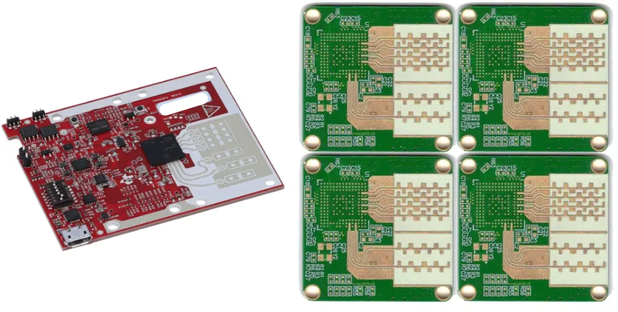
Selecting an antenna PCB approach requires deciding three things before fabrication: the antenna structure, the PCB material stack-up, and the manufacturing controls needed to preserve RF performance. Engineers should evaluate frequency band, impedance requirements, antenna clearance, dielectric properties, and supplier verification data before releasing designs. Procurement teams should request controlled impedance evidence, stack-up documentation, and RF validation records rather than comparing PCB suppliers only by board price.
For wireless products using Bluetooth, Wi-Fi, RFID, LoRa, IoT, automotive, or medical connectivity, antenna performance depends on the complete PCB system. The copper geometry, substrate, ground plane, enclosure, and manufacturing process all influence the final communication range and reliability.
What is an antenna PCB and when should engineers choose one?
An antenna PCB integrates the antenna directly into the printed circuit board using copper structures that radiate electromagnetic signals. Compared with standalone antennas, PCB antennas can reduce component count, simplify assembly, and support compact product designs.
Common PCB antenna structures include:
- Monopole and dipole antennas
- Inverted-F antennas (IFA / PIFA)
- Meandered line antennas
- Patch and microstrip antennas
- Fractal antennas for broadband applications
The correct antenna type depends on the wireless requirement, available board area, mechanical environment, and manufacturing capability. A 2.4 GHz Wi-Fi or Bluetooth product typically requires different antenna decisions than a sub-GHz LoRa or RFID design. GNSS receivers are another case, covered in our GPS PCB guide.
Engineers should decide whether the antenna should be:
- A printed trace antenna integrated into the PCB
- A chip antenna mounted on the PCB
- An external antenna connected through an RF feed structure
A printed antenna minimizes additional components but requires careful control of PCB geometry and surrounding materials. A chip antenna can simplify the RF design but introduces component selection constraints. External antennas provide flexibility but require mechanical integration.
What PCB material should be selected for antenna performance?
The PCB dielectric directly affects antenna behavior because electromagnetic fields interact with the substrate. Important material parameters include dielectric constant (Dk), dielectric loss factor (Df), thickness, copper weight, and surface characteristics.
Standard FR-4 can support many wireless applications, but high-frequency antenna PCBs often require specialized laminates such as Rogers, Taconic, or PTFE-based materials when lower signal loss and tighter RF consistency are required.
The material decision should be based on:
- Operating frequency
- Required antenna efficiency
- RF loss budget
- Mechanical constraints
- Production repeatability
Typical industry reference values:
| PCB parameter | Typical engineering range | Design risk if uncontrolled | Evidence to request |
|---|---|---|---|
| RF impedance | 50 ohms target, commonly controlled within approximately ±10% for many RF designs | Reflections, mismatch, reduced transmission efficiency | Controlled impedance report and test coupon data |
| High-frequency laminate Dk | Approximately 2.5-4.5 for many RF laminate families | Resonance shift and antenna detuning | Material certificate and laminate datasheet |
| FR-4 dielectric constant | Approximately 3.8-4.8 depending on resin system and test method | Antenna tuning variation between suppliers | Stack-up confirmation and material specification |
| Dielectric loss tangent (Df) | Approximately 0.001-0.02 depending on laminate type | Higher RF attenuation | Material datasheet at target frequency |
| Copper weight | Common PCB values include 0.5 oz, 1 oz, and 2 oz copper | Changes trace geometry and RF behavior | Copper weight specification in fabrication drawing |
| RF trace width tolerance | Typical production capability is approximately ±0.05 mm to ±0.10 mm depending on process | Impedance variation and feed-line mismatch | Cross-section measurement report |
Material selection should be finalized with the PCB manufacturer before fabrication because the same nominal laminate name can produce different electrical results when thickness, copper, and stack-up construction change.
How should engineers select antenna PCB materials by frequency?
Material selection directly controls antenna efficiency, detuning risk, and production repeatability. The table below maps common high-frequency laminates to their usable frequency range, dielectric properties, and relative cost so engineers can narrow the candidate list before requesting supplier quotes.
| Material | Dk | Df @ 10 GHz | Best frequency range | Typical application | Cost relative |
|---|---|---|---|---|---|
| Rogers RO4003C | 3.38 | 0.0027 | <20 GHz | RF antennas | High |
| Rogers RO4350B | 3.48 | 0.0037 | <30 GHz | 5G antennas | High |
| Rogers RO3003 | 3.0 | 0.0010 | <30 GHz | mmWave | High |
| RT/dupont 5880 | 2.20 | 0.0009 | <40 GHz | Microwave | Very high |
| Taconic TLY-5 | 2.22 | ~0.0019 | <30 GHz | High-frequency | High |
| Standard FR-4 | 4.3–4.7 | 0.020 | <2 GHz | Low-cost / consumer | Low |
For designs operating below 2 GHz, standard FR-4 is often sufficient and avoids the cost premium of specialized laminates. Above 2 GHz, the rising loss tangent of FR-4 makes Rogers, Taconic, or PTFE-based materials the safer choice. Engineers should confirm the selected laminate's Dk and Df at the actual operating frequency with the manufacturer, because published values can vary with thickness, copper foil, and test method.
How should antenna PCB impedance and RF feed lines be designed?
The antenna feed network must transfer energy efficiently between the radio circuit and the antenna element. Most antenna PCB designs use a 50 ohm impedance target between the RF component and antenna.
Common feed structures include:
- Microstrip transmission lines
- Coplanar waveguide (CPW) structures
- Grounded RF transmission structures
The RF feed design depends on:
- Trace width
- Copper thickness
- Dielectric thickness
- Dk value
- Reference plane location
A PCB manufacturer should receive the final stack-up requirements before quoting because impedance cannot be controlled accurately without defined dielectric thickness and material properties.
Engineers should also include tuning provisions such as matching components. A typical RF matching network may use inductors and capacitors to compensate for antenna and enclosure effects after prototype testing.
How does antenna clearance and ground plane layout affect wireless range?
Antenna performance depends heavily on the surrounding PCB area. The antenna should normally be placed near the PCB edge or corner, with clearance from batteries, metal shields, connectors, and large conductive structures.
Important layout controls include:
- Antenna keep-out areas
- Ground plane boundaries
- Component placement restrictions
- RF trace routing discipline
The ground plane acts as part of the antenna system. Incorrect ground geometry can shift resonance, reduce efficiency, and increase tuning effort.
For compact wireless products, the final enclosure must be considered early. A design that performs correctly on a bare PCB can change after adding:
- Metal housings
- Batteries
- Displays
- Mechanical brackets
- Nearby cables
What are the antenna design challenges in metal enclosures?
Antenna design challenges in metal enclosures are the dominant cause of wireless-range failures once a working bare-PCB prototype moves into a final product. Metal acts as a near-field reflector and absorber; a plastic or FR-4 PCB region that radiated cleanly on the bench can lose half its efficiency or detune by tens of megahertz once it sits inside a metal housing, near a metal bracket, or next to a metal-shielded display flex.
The three physical effects that drive antenna design challenges in metal enclosures:
- Reflection and image-plane shift — A nearby metal surface creates an image antenna at the mirror plane, changing the effective electrical length. The shift depends on the gap between the radiator and the metal. A 2 mm gap at 2.4 GHz is enough to move the resonance noticeably; a 6 mm gap is often required for a clean match.
- Field blocking — A metal wall between the radiator and free space reduces the antenna's effective aperture. Slot, IFA, and patch antennas are more tolerant of nearby conductors than monopole or dipole structures; selection at the start of the project avoids the worst-case geometry.
- Coupling into nearby metal traces and flex — Display flex, battery tab, and metal-shielded connectors re-radiate energy and distort the pattern. Keep-out zones around the antenna and dedicated ground return paths prevent the worst symptoms.
Engineering practice to handle antenna design challenges in metal enclosures:
- Define the enclosure geometry and the antenna keep-out zone before gerber release; a 4–6 mm non-conductive gap between the PCB antenna edge and any metal wall is a safe starting range for sub-6 GHz designs.
- Specify the enclosure material (plastic, painted metal, conductive plastic) and any conductive gasket around the radiator window. Conductive plastic windows attenuate the antenna more than painted metal with a true plastic window.
- Run an electromagnetic simulation with the enclosure model — bare-PCB patterns rarely survive the housing; include the housing file in HFSS, CST, or ADS before committing the layout.
- Add a tuning network (π or L matching) so the engineer can compensate for the shift once the prototype is built; a fixed-geometry antenna without tuning margin is the most expensive mistake.
- Verify with VNA and anechoic-chamber or range tests in the final housing; do not accept "PCB tunes on the bench" as a sign-off.
If the enclosure cannot be redesigned to give the antenna clearance, evaluate an off-board antenna (cable-fed patch or chip antenna mounted through the housing) before adding the policy. Many designs that fail as PCB antennas work as external antennas connected through an RF feed.
What manufacturing capabilities should an antenna PCB supplier provide?
Antenna PCB fabrication requires more than standard digital PCB production. The supplier should demonstrate control over RF-specific manufacturing variables.
Important manufacturing capabilities include:
- Controlled impedance processing
- Consistent laminate handling
- Tight trace width and spacing control
- RF surface finish control
- Stack-up documentation
- Optical inspection of RF features
High-frequency antenna designs may require low-loss laminates, hybrid FR-4/RF constructions, and controlled manufacturing processes to maintain repeatability between prototype and production builds.
Manufacturing review should include:
- PCB layer stack-up approval
- RF trace geometry verification
- Antenna keep-out verification
- Via placement review
- Final electrical testing requirements
Which antenna PCB failures occur most often and how can they be diagnosed?
| Failure mode | Common root cause | Verification method |
|---|---|---|
| Antenna frequency shift | Incorrect Dk, changed PCB thickness, nearby metal, or enclosure effects | Compare simulation results with VNA measurements and review final stack-up |
| Poor wireless range | Insufficient antenna clearance, incorrect ground plane, or inefficient antenna geometry | Measure antenna performance and inspect mechanical integration |
| RF signal loss | High dielectric loss, poor material selection, or unsuitable feed routing | Review laminate Df data and measure RF path performance |
| Impedance mismatch | Incorrect trace width, dielectric thickness variation, or stack-up changes | Request impedance test coupon results |
| Prototype works but production fails | Manufacturing variation or inconsistent material/process control | Compare production cross-section reports and RF measurements |
What antenna PCB design practices improve production success?
A reliable antenna PCB workflow begins before layout completion.
Recommended engineering practices include:
- Use electromagnetic simulation tools such as CST, HFSS, or ADS during antenna development.
- Keep RF traces short and avoid unnecessary vias or trace stubs.
- Maintain consistent reference planes for RF transmission lines.
- Include tuning components for antenna matching.
- Validate antenna behavior in the final mechanical enclosure.
- Review antenna detuning risks caused by nearby materials.
Simulation reduces design iterations, but physical validation remains necessary because the final product environment affects antenna behavior.
How should engineers prepare an RFQ for antenna PCB manufacturing?
A complete RFQ package helps suppliers evaluate manufacturability and provide meaningful technical feedback.
Submit these files and specifications:
- Gerber files or ODB++ manufacturing data
- Bill of materials (BOM)
- PCB fabrication drawing
- PCB stack-up requirements
- Material requirements including Dk and Df targets when specified
- Layer definition files
- Drill files
- Via drawing
- Controlled impedance requirements
- Copper weight requirements
- Surface finish requirements
- Antenna keep-out drawings
- Mechanical enclosure information if available
- Assembly drawings for antenna-related components
Request these supplier evidence documents:
- Proposed PCB stack-up
- Material datasheets
- Controlled impedance report
- Test coupon results
- Cross-section report
- Copper thickness verification
- RF inspection records
- Electrical test documentation
- Manufacturing capability review for antenna clearance and RF geometry
For RF products, supplier communication before tooling is often more valuable than correcting antenna problems after production begins.
How do antenna PCB options compare for wireless product decisions?
| Design choice | Engineering benefit | Main tradeoff | Best fit |
|---|---|---|---|
| PCB trace antenna | Lowest additional component count and full integration | Requires antenna tuning and careful layout control | IoT sensors, Bluetooth devices, compact wireless products |
| Chip antenna | Small footprint and simplified antenna geometry | Requires component selection and matching network design | Space-limited consumer devices |
| External antenna | Predictable placement and strong mechanical flexibility | Adds components and mechanical requirements | Gateways, industrial systems, long-range applications |
| High-frequency laminate PCB | Better RF consistency at higher frequencies | Higher material complexity than standard FR-4 | RF, microwave, advanced wireless systems |
Conclusion: What should be decided before ordering an antenna PCB?
Antenna PCB success depends on selecting the right antenna architecture, controlling the RF stack-up, and verifying that the PCB manufacturer can reproduce the intended electrical characteristics.
Before production, engineers should confirm:
- Operating frequency requirements such as 2.4 GHz Wi-Fi/Bluetooth or sub-GHz wireless bands
- 50 ohm RF feed requirements
- Antenna clearance and ground plane rules
- PCB material Dk and Df specifications
- Manufacturing verification requirements
At Highleap PCB Factory, antenna PCB manufacturing combines RF PCB production knowledge with PCB assembly capability to support wireless designs from prototype development through volume manufacturing.
For more information on RF and antenna PCB production capabilities, visit our PCB manufacturing services.