
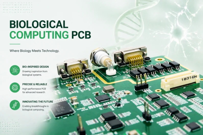
A biological computing PCB is a printed circuit board designed to connect living cells, biological fluids, biosensors, microelectrodes or microfluidic structures to electronic measurement, stimulation and control circuits. It is not only a circuit carrier; it is a wet-dry interface where electrical noise, ionic contamination, corrosion, cell compatibility, leakage paths and regulatory scope have to be reviewed together.
This guide is written for engineering teams building bioelectronic interface boards, biosensor array PCBs, neural interface carrier boards, organ-on-chip electronics and lab-on-chip control boards. It focuses on board-level decisions that can be specified in a PCB or PCBA package before prototypes are released.
Key Takeaways
- Biological computing PCB design starts with the contact boundary: which areas touch fluid, cells, tissue, electrodes, gaskets, adhesives or sterilization processes.
- Low-noise recording is a system target, not a laminate slogan. Guarding, grounding, amplifier placement, power sequencing, shielding and cleaning all affect microvolt-level measurements.
- A microelectrode array carrier board should be reviewed as a fine-pitch interconnect problem plus an electrochemical interface problem.
- Parylene C, SU-8, noble-metal electrodes, high-Tg laminates and halogen-free materials can be useful, but they do not automatically make a medical device biocompatible.
- For medical, implantable or patient-contact projects, the PCB supplier can support materials, traceability and process documentation; final biological safety, clinical performance and regulatory submission remain device-level responsibilities.
- The strongest RFQ package includes the wet-zone map, electrode materials, expected signal range, fluid chemistry, sterilization plan, test method and acceptance criteria.
In This Guide
- What is a biological computing PCB?
- Where biological computing PCBs are used
- Wet-dry interface architecture
- Low-noise recording and stimulation layout
- Microelectrode array carrier board design
- Lab-on-chip and microfluidic PCB integration
- Biocompatible materials, cleaning and sterilization
- Common failure modes and review checks
- Cost drivers in biological computing PCB manufacturing
- RFQ checklist
- Why work with HILPCB
- Reference standards and specifications
- FAQ
What is a biological computing PCB?
A biological computing PCB supports electronic interaction with biological systems. The board may record neural spikes, drive stimulation pulses, monitor cell-culture impedance, control a microfluidic pump, heat an organ-on-chip zone to physiological temperature, or route thousands of microelectrode signals to amplifiers and data converters.
The board-level problem is different from ordinary industrial electronics for three reasons.
First, biological media are conductive. Saline, buffer solution, culture medium and bodily fluids can create leakage paths between exposed conductors. A spacing rule that is safe in dry air may fail when ionic liquid bridges the surface.
Second, biological signals are small. EEG, extracellular spikes, impedance changes and electrochemical sensor currents can sit in the microvolt, millivolt, nanoampere or picoampere range depending on electrode type and bandwidth. Layout noise, flux residue, input leakage and power ripple can become the signal.
Third, biological compatibility is a system property. A lead-free solder joint, a gold finish or a Parylene C coating may be part of a biocompatibility strategy, but none of those items alone proves that a completed device is safe for cells, tissue or patients. The actual contact type, duration, extraction method, sterilization method and use environment must be defined at the device level.
That makes the best design question very practical: what exactly touches biology, for how long, under what voltage, in which fluid, and what measurement or stimulation result must remain stable?
Where biological computing PCBs are used
The phrase biological computing PCB can describe several neighboring applications. They share wet-dry interface challenges, but they should not be treated as one manufacturing route.
| Application | Typical board role | Main PCB risk | What to define early |
|---|---|---|---|
| Neural interface carrier board | Route microelectrode or connector signals to amplifiers, ADCs and stimulation channels | Noise, crosstalk, leakage and connector density | Electrode count, signal bandwidth, input impedance, stimulation limits and shielding plan |
| MEA carrier board | Fan out dense electrode arrays from a chip, glass MEA or custom sensor array | Fine-pitch routing, passivation alignment and electrode exposure | Pad pitch, trace/space, via strategy, exposed electrode finish and wet-zone map |
| Biosensor array PCB | Host electrochemical, optical or impedance sensors for biological samples | Contamination, drift and cross-sensitivity | Target analyte, electrode material, test medium, calibration method and cleaning limit |
| Lab-on-chip PCB | Provide electrical sensing, heating and actuation under a microfluidic cartridge | Fluid leakage, adhesion failure and thermal non-uniformity | Microfluidic footprint, gasket compression, bonding surface and heater/sensor locations |
| Organ-on-chip electronics | Support culture monitoring, pump/valve control and temperature regulation | Long-duration wet operation and incubator exposure | Culture duration, humidity, CO₂ exposure, sterilization plan and connector protection |
| Wearable biopotential board | Record ECG, EMG, EEG or other skin-contact signals | Motion artifact, input protection and skin-contact safety | Electrode type, patient isolation boundary, IEC scope and enclosure interface |
| Implant-adjacent or implantable electronics | Interface with tissue, leads or implantable arrays | Biological safety, hermeticity, traceability and regulatory burden | Contact duration, patient-contact category, sterilization method and regulatory owner |
A single article cannot certify a board for all of these uses. The same PCB stack-up may be acceptable for a disposable lab cartridge and completely unsuitable for a long-term implant. The RFQ and design review should therefore classify the project before material selection begins.
Wet-dry interface architecture
The wet-dry interface is the first architecture decision. In biological electronics, the question is not simply whether the PCB has a conformal coating. The question is which features are intentionally exposed, which features must never see fluid, and how fluid movement is mechanically controlled.
A good wet-zone drawing separates the board into at least four regions:
| Region | Typical features | PCB design objective | Review questions |
|---|---|---|---|
| Exposed biological contact | Electrodes, sensing pads, stimulation contacts, reference electrodes | Stable electrochemical contact with controlled geometry | What finish is exposed? What is the electrode area? What current density or measurement range is expected? |
| Passivated wet zone | Traces beneath fluid chamber, coated copper, sealed vias | Prevent ionic leakage and corrosion while allowing selected openings | What coating is used? What thickness range and pinhole test are specified? |
| Mechanical sealing zone | Gasket land, adhesive bond line, cartridge compression area | Maintain leak-free boundary without stressing components | What surface flatness and solder mask restrictions are required? |
| Dry electronics zone | Amplifiers, ADCs, MCU, connectors, power supplies, wireless modules | Keep sensitive electronics isolated from fluid and condensation | What creepage, shielding, cleaning and connector protection are required? |
For many prototypes, a practical starting point is to keep exposed conductors in the wet zone widely spaced, often far beyond ordinary dry-environment PCB clearance. The final value should be validated against fluid conductivity, applied voltage, exposure duration, coating integrity and contamination level. A fixed spacing number without those conditions is not a reliable release rule.
Passivation also needs to be reviewed as geometry. A coating specification such as Parylene C, 5-15 μm is incomplete unless it defines masking, exposed electrode openings, adhesion preparation, inspection method and rework limits. A small coating defect can create a leakage path that appears only after hours or days in warm saline.
Common wet-dry design controls include:
- keep the analog front end outside the wet chamber whenever possible;
- avoid placing vias directly under fluid unless they are fully sealed and validated;
- use guard rings around high-impedance nodes where leakage current matters;
- isolate reference electrode routing from noisy stimulation or pump-driver paths;
- define gasket compression areas without exposed copper, tall components or solder mask defects;
- specify post-assembly cleaning and dry-pack handling when surface leakage is a risk.
The strongest layout reviews mark wet zones directly on the fabrication drawing, not only in an email or 3D model. That prevents coating, solder mask, surface finish and assembly teams from guessing which copper features are biological interfaces.
Low-noise recording and stimulation layout
Low-noise biological recording depends on the entire signal chain. The PCB cannot make a noisy electrode quiet, but it can easily ruin a good electrode with leakage, capacitive coupling or power ripple.
For neural, EEG, EMG, ECG, impedance and electrochemical front ends, the first review item is the signal definition. The design package should state the signal amplitude range, bandwidth, source impedance, reference scheme, common-mode range and expected environmental interference. A low-noise PCB request without those values is too vague to quote accurately.
Board-level design controls for low-noise biological signals
| Design area | Recommended review action | Why it matters |
|---|---|---|
| Amplifier placement | Place the first gain stage close to the electrode connector or sensing pads where mechanically possible | Long high-impedance traces collect capacitive noise and leakage current |
| Ground strategy | Use a continuous analog reference plane and define the single-point connection to digital or chassis ground | Split planes and accidental return paths can inject digital noise into microvolt-level signals |
| Guarding | Guard high-impedance input nodes with driven guard traces where the amplifier architecture supports it | Guarding reduces leakage and parasitic capacitance at sensitive nodes |
| Power tree | Use low-noise LDOs for analog front ends; filter switching rails before analog regulation | Switching noise can appear directly as measurement noise or stimulation artifact |
| Digital isolation | Route clocks, SPI, I²C, USB, Ethernet and wireless sections away from electrode inputs | Fast edges couple through capacitance, return currents and ground bounce |
| Shielding | Use grounded shields, via fences and enclosure-level shielding where needed | Incubator motors, pumps, LED drivers and wireless radios can couple into sensor wiring |
| Cleaning | Define no-clean vs cleaned process intentionally; verify ionic residues when leakage matters | Flux residue and moisture can create input leakage paths |
| Test coupon | Include SIR, impedance or leakage test structures for high-risk wet-zone builds | Process drift is easier to catch on a repeatable coupon than on a biological assay |
Stimulation paths need a separate review. A board that can record a small signal may not be safe or clean enough to deliver stimulation pulses. Stimulation routing must control parasitic capacitance, charge injection, return path, blanking time and protection devices. The acceptance criteria should be defined by the device designer because tissue, cells and electrodes can have very different safe operating limits.
For simultaneous stimulation and recording, design teams should plan for artifact management from the beginning. Physical separation helps, but it is not enough by itself. The blanking strategy, amplifier recovery time, electrode polarization and firmware timing all influence whether the measured signal is real biology or a stimulation artifact.
Microelectrode array carrier board design
A microelectrode array carrier board connects dense electrode sites to external electronics. The MEA itself may be a silicon, glass, ceramic or polymer structure, while the PCB provides fan-out, shielding, mechanical registration, connectors, stimulation routing and sometimes the first amplification stage.
The routing problem usually looks simple in block diagrams and difficult in layout. A few dozen electrode channels may be manageable on a conventional multilayer board. Hundreds or thousands of channels can force HDI PCB construction, sequential lamination, microvias, fine trace/space, tight solder mask registration and custom connector strategy.
MEA carrier board decision table
| Decision | Low-complexity route | Higher-complexity route | What drives the choice |
|---|---|---|---|
| Channel count | 16-64 channels | 128-4,096+ channels | Electrode density, connector style and amplifier architecture |
| Interconnect | Standard connector or flex tail | Fine-pitch BGA, anisotropic film, custom socket or wire bond | MEA package, pitch and serviceability |
| Routing | Standard multilayer fan-out | HDI with microvias and fine-line routing | Pad pitch, channel count and shielding requirements |
| Electrode exposure | Pre-made MEA handles biological interface | PCB has exposed sensing/stimulation electrodes | Whether the PCB itself contacts cells or fluid |
| Amplifier location | Off-board instrument front end | On-board low-noise front end close to electrodes | Signal amplitude, cable length and environmental noise |
| Stimulation | Separate stimulator path | Integrated stimulation/recording switching | Artifact tolerance, charge balancing and safety controls |
If the PCB includes exposed electrodes, finish selection becomes critical. Gold can be useful for many biosensor and low-current contact applications, while platinum, platinum-iridium, iridium oxide, PEDOT-based coatings or other specialized electrode systems may be selected for specific electrochemical or stimulation requirements. The PCB drawing should not simply say biocompatible finish. It should name the exposed material, surface area, roughness or coating requirement where relevant, and the inspection method.
Registration is another common hidden risk. A passivation opening that is slightly shifted may still look acceptable under normal PCB inspection but fail as an electrode because the active area changed. For dense arrays, the design should define passivation-opening tolerance, fiducial strategy and optical inspection requirements.

Lab-on-chip and microfluidic PCB integration
A lab-on-chip PCB may support sensing, heating, pumping, valve control, optical alignment and data acquisition under a disposable or reusable fluidic cartridge. The PCB often becomes both an electrical platform and a mechanical datum.
The most important decision is whether the microfluidic channel is permanently bonded to the PCB, mechanically clamped with a gasket, or separated into a replaceable cartridge. Each route changes PCB requirements.
| Integration route | Advantage | PCB risk | Typical review item |
|---|---|---|---|
| Bonded PDMS or glass channel | Compact and direct sensor access | Bond-line failure, surface contamination, rework difficulty | Surface flatness, solder mask exclusion, plasma/bonding compatibility |
| Gasket-compressed cartridge | Replaceable and easier to service | Compression set, leakage, uneven pressure | Gasket land width, screw pattern, torque limit, support ribs |
| Disposable cartridge over reusable PCB | Protects electronics from sample contamination | Alignment and contact repeatability | Spring contacts, pogo pins, fiducials and fluidic seal verification |
| PCB-integrated heater and sensor | Tight thermal control near culture zone | Hot spots and measurement drift | Copper heater geometry, thermistor placement, thermal simulation |
| Pump/valve driver PCB | Strong system integration | EMI and inductive switching noise | Flyback protection, ground separation and sensor shielding |
For cell-culture systems, 37°C temperature control is often a target, but the required tolerance depends on the assay. A heater trace on a PCB should not be described as sufficient until the full assembly has been tested with the cartridge, fluid flow, incubator or ambient environment, enclosure and sensor calibration in place. A thermal model is useful, but a wet functional test usually decides whether the board is stable enough for the biological protocol.
Microfluidic designs also create cleaning and sterilization questions. A PCB that works in dry benchtop electronics may fail after repeated ethanol wipe-down, UV exposure, autoclave cycles, condensation or incubator humidity. The board package should specify the actual cleaning and sterilization exposure instead of using broad phrases such as sterilizable PCB.
Biocompatible materials, cleaning and sterilization
Biocompatibility should be treated as a risk-based device-level evaluation. At PCB level, the supplier can help control materials, residues, surface finish, coatings, traceability and process documentation. The completed device still needs biological evaluation based on contact type and contact duration.
For non-patient research systems, the acceptance criteria may be cell viability, signal drift, leakage current and assay repeatability. For patient-contact or implantable systems, the acceptance criteria may include ISO 10993 biological endpoints, sterilization validation, packaging, traceability and regulatory documentation. Those two projects should not use the same release language.
Material and process options to review
| Topic | Possible PCB-level control | Important limitation |
|---|---|---|
| Lead-free assembly | SAC-series lead-free solder and controlled component selection | Lead-free does not automatically mean cytotoxicity-free |
| Halogen-free laminate | Halogen-free FR-4 or specialty laminate where required | Electrical, moisture and thermal performance still need validation |
| Surface finish | ENIG, electrolytic gold, hard gold, platinum or other specified electrode finish | Only the exposed biological contact finish matters for cell/fluid interaction |
| Conformal coating | Parylene C, selected medical-grade coating or assay-compatible coating | Coating must define masking, adhesion, thickness, pinhole inspection and sterilization compatibility |
| Solder mask | Biocompatibility-reviewed or excluded from wet contact where needed | Standard solder mask is not automatically suitable for direct culture contact |
| Cleaning | Aqueous cleaning, solvent compatibility review, ionic contamination test or ion chromatography | A single ROSE number does not prove biological safety |
| Sterilization | Material review for autoclave, ethylene oxide, gamma, e-beam, UV or alcohol exposure | Each method can affect polymers, adhesives, coatings, connectors and components differently |
| Traceability | Lot traceability for laminate, finish, coating, solder paste and critical components | Traceability supports documentation; it does not replace device validation |
A common historical ionic cleanliness screen is 1.56 µg/cm² NaCl equivalent, but high-risk biological interfaces often need more specific process qualification, such as ion chromatography, surface insulation resistance, soak testing, electrochemical drift testing or extractables/leachables review. The right method depends on the biology, the fluid and the regulatory path.
For autoclave exposure, a high-Tg laminate alone is not enough. The connector, solder mask, coating, adhesive, sensor material, component package and moisture absorption behavior all matter. If repeated 121°C steam sterilization is required, it should be specified as a validated assembly requirement, not assumed from a laminate data sheet.
Common failure modes and review checks
A useful biological computing PCB review should predict failures before the first wet test. Many problems do not appear in bare-board electrical test because they only emerge after fluid exposure, humidity, temperature, stimulation pulses or biological incubation.
| Failure mode | What usually causes it | Early warning sign | PCB-level prevention |
|---|---|---|---|
| Ionic leakage between electrodes | Wet residue, inadequate spacing, coating defect or saline bridge | Baseline drift, unexplained DC offset, noisy low-frequency channel | Wet-zone spacing review, guard rings, cleaning validation, soak test |
| Copper corrosion | Exposed copper, coating pinhole or failed passivation edge | Green/blue discoloration, rising impedance, intermittent signal | Noble-metal exposure, sealed copper, passivation inspection |
| Cell toxicity | Flux residue, incompatible solder mask, unqualified adhesive or leachable material | Poor cell attachment or viability loss near the board | Material selection, extraction testing, cleaning and cytotoxicity review |
| Amplifier saturation | Electrode polarization, input bias current, reference instability or stimulation artifact | Flatlined channel or slow recovery after pulse | Reference design review, input protection, blanking and recovery testing |
| Crosstalk between channels | Dense parallel routing, poor shielding or shared return path | Same artifact appears on neighboring channels | Ground shielding, route separation, driven guards and layout symmetry |
| Fluid leakage into dry zone | Gasket land error, warped board, adhesive failure or over-compression | Condensation, intermittent connector faults, current spikes | Mechanical seal design, flatness control, torque specification |
| Heater hot spot | Poor copper distribution, sensor placed away from culture zone or inadequate model | Local cell stress or assay drift | Thermal simulation, IR mapping, wet thermal test |
| Sterilization damage | Material not compatible with steam, radiation, gas or solvent | Delamination, coating cracks, brittle connector or drift | Sterilization method specified before material freeze |
| Surface contamination after assembly | Incomplete cleaning or unsuitable no-clean flux | High leakage, drift after humidity exposure | Cleaning process validation and contamination test plan |
| Connector intermittency | Wet exposure, corrosion, cable strain or repeated cartridge insertion | Channel dropout during handling | Connector sealing, strain relief and insertion-cycle testing |
This table is more valuable than a generic capability list because it turns the review into a release checklist. If a design cannot say how each high-risk failure is prevented or tested, it is not ready for a wet biological prototype.
Cost drivers in biological computing PCB manufacturing
Biological computing PCBs become expensive when the project combines fine geometry, wet-zone control, coating, specialty finish and low-volume validation. Cost usually comes from the number of controlled interfaces, not from the phrase bioelectronic.
| Cost driver | Why it increases cost | How to manage it |
|---|---|---|
| HDI and fine-line routing | Sequential lamination, microvias and tighter registration raise process complexity | Separate dense electrode fan-out from lower-density control electronics where possible |
| Specialty electrode finish | Noble metals and electrochemical coatings require controlled exposure and inspection | Use specialty finish only where biology contacts the board |
| Parylene or selective coating | Masking, coating thickness control and pinhole inspection add steps | Provide an exact coating keep-out and exposed-pad map |
| Wet-zone validation | Soak tests, impedance drift, leakage and visual inspection take time | Define acceptance criteria before fabrication |
| Low-noise assembly | Cleaning, shielding and power-tree review may require extra test fixtures | Include test pads and known-good measurement setup in the design |
| Custom fixtures or cartridges | Microfluidic alignment and sealing may need mechanical tooling | Freeze interface dimensions early and use replaceable cartridge logic where possible |
| Documentation and traceability | Medical or regulated programs need controlled records | State documentation level in the RFQ instead of adding it after quote |
The cheapest route is not always a standard PCB. If the board will be rebuilt many times because wet-zone assumptions were missing, an initially lower fabrication price can become the expensive path. For biological interfaces, the more useful cost question is: which risk must be eliminated on the first prototype, and which can wait for the second build?
RFQ checklist
A biological computing PCB quote is much more accurate when the supplier receives both electrical and biological interface data. The following checklist can be copied into an RFQ package.
1. Board files and manufacturing data
- Gerber or ODB++ files
- NC drill files
- Stack-up requirement or target thickness
- Controlled impedance requirements, if any
- IPC class requirement
- Board outline, panelization preference and fiducials
- Assembly drawing and pick-and-place file
- Bill of materials with approved alternates
- Test-point map and programming requirements
2. Wet-zone and biological interface data
- Wet-zone map showing all fluid-contact areas
- Electrode material and surface finish
- Exposed electrode geometry and passivation openings
- Fluid chemistry, conductivity, pH and expected exposure time
- Cell type, tissue type or sample type if relevant to material compatibility
- Expected temperature, humidity, CO₂, vibration and handling conditions
- Gasket, cartridge, PDMS, glass or adhesive interface drawings
- Cleaning, sterilization or disinfection method
3. Electrical performance data
- Signal type: voltage, current, impedance, electrochemical, optical or stimulation
- Signal amplitude range and bandwidth
- Source impedance and reference electrode scheme
- Input-referred noise target and measurement bandwidth
- Stimulation pulse amplitude, duration, frequency and charge-balance requirement
- Power rails, ripple limits and sequencing requirements
- Digital interfaces: SPI, I²C, USB, Ethernet, BLE, Wi-Fi or custom bus
- Shielding, grounding and enclosure constraints
4. Validation and documentation data
- Required soak test duration and medium
- Impedance drift or leakage-current acceptance criteria
- Ionic contamination or ion chromatography requirement
- Coating thickness and pinhole inspection method
- Cytotoxicity, extractables/leachables or ISO 10993 test plan if applicable
- Sterilization validation responsibility
- Traceability level and certificate requirements
- Prototype quantity and target production volume
Why work with HILPCB
Biological computing boards sit between HDI PCB, multilayer PCB, high-speed PCB, SMT assembly and controlled surface-finishing work. HILPCB can support the PCB and PCBA manufacturing side of that interface by reviewing the build around manufacturability, wet-zone definition, low-noise layout risks, coating keep-outs, cleaning requirements and assembly constraints.
For early prototypes, the most useful support is often a design-for-manufacturing and design-for-test review before the first board is built. Fine-pitch MEA routing, electrode exposure, selective coating, gasket land geometry and amplifier placement are much easier to correct before fabrication.
For production-oriented projects, the review can shift toward repeatability: stack-up control, impedance control, material traceability, assembly inspection, test fixtures, coating inspection and documented cleaning processes. When the product is medical or patient-contacting, HILPCB can provide PCB/PCBA manufacturing documentation that supports the customer’s device-level technical file, while the customer’s regulatory and quality teams remain responsible for final biological safety, clinical performance and submission strategy.
Send the wet-zone map, Gerber package, BOM, electrode requirements and validation plan through the Quote page so the engineering team can review the build as a biological interface instead of a standard dry-environment PCB.
Reference standards and specifications
The following standards and specifications are relevant to many biological computing PCB projects, but applicability depends on the device category, contact type, geography and regulatory path.
- ISO 10993-1 — Biological evaluation of medical devices, risk management framework
- ISO 10993-5 — Tests for in vitro cytotoxicity
- ISO 10993-12 — Sample preparation and reference materials
- ISO 10993-17 — Toxicological risk assessment of medical device constituents
- ISO 10993-18 — Chemical characterization of medical device materials
- USP <87> — Biological reactivity tests, in vitro
- USP <88> — Biological reactivity tests, in vivo
- IPC-2221 — Generic standard on printed board design
- IPC-6012 — Qualification and performance specification for rigid printed boards
- IPC-A-610 — Acceptability of electronic assemblies
- IPC J-STD-001 — Requirements for soldered electrical and electronic assemblies
- IPC-TM-650 2.3.25 — Resistivity of solvent extract test method
- IEC 60601-1 — Medical electrical equipment, basic safety and essential performance, when device scope applies
FAQ
What is a biological computing PCB?
A biological computing PCB is a circuit board designed to interface electronics with living cells, tissue, biological fluid, biosensors, microelectrodes or microfluidic systems. It must manage wet-dry isolation, low-noise measurement, electrochemical stability, material compatibility and validation requirements.
Why can’t a standard PCB be used directly in saline or cell culture?
Standard PCBs are designed mainly for dry environments. Saline and culture media are conductive and can cause leakage, corrosion and contamination if copper, residues, solder mask, vias or components are not properly isolated from the wet zone.
Is Parylene C enough to make a PCB biocompatible?
No. Parylene C can be a useful barrier coating, but biocompatibility depends on the finished device, coating coverage, adhesion, pinholes, exposed materials, cleaning, sterilization and biological evaluation. The use case and contact duration determine the required test plan.
What is the biggest PCB challenge in MEA carrier boards?
The biggest challenge is combining dense electrode fan-out with low-noise routing and stable biological contact. The carrier may need HDI routing, tight registration, controlled passivation openings, shielding and a connector strategy that does not compromise signal quality.
How should a low-noise biosignal PCB be specified?
Specify the signal amplitude, bandwidth, source impedance, input-referred noise target, reference scheme, power ripple limit, shielding requirement and measurement method. Without those values, low-noise is not specific enough for manufacturing or validation.
Are biological computing PCBs always medical devices?
No. Many biological computing PCBs are research, laboratory, environmental sensing or life-science instrumentation boards. A board becomes part of a medical device context when the finished product’s intended use, patient contact and regulatory claims place it there.
What should be included in a biological computing PCB RFQ?
Include Gerber or ODB++ files, BOM, stack-up, wet-zone map, electrode material, fluid chemistry, signal range, coating requirement, sterilization method, validation criteria and documentation needs. The wet-zone map is especially important because it tells the manufacturer what is allowed to contact biology.
Next step
If your design includes exposed electrodes, cell-culture media, microfluidic sealing, MEA fan-out or microvolt-level recording, treat the quote as a biological interface review rather than a normal PCB build. Upload your files through the Quote page and include the wet-zone map, electrode requirements and validation plan so HILPCB can review manufacturability, assembly risk and test strategy before the first prototype.