HILPCB delivers professional Bluetooth PCB manufacturing and assembly solutions for wireless communication devices across consumer electronics, IoT applications, and industrial systems. Our specialized Bluetooth PCB services enable reliable short-range wireless connectivity with exceptional RF performance and power efficiency.
Modern Bluetooth devices require sophisticated PCB designs integrating Bluetooth modules, antenna systems, power management, and host processors within compact form factors. Our expertise encompasses Bluetooth Classic, Bluetooth Low Energy (BLE), and advanced Bluetooth 5.x implementations supporting diverse wireless applications.
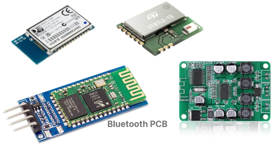
Bluetooth PCB Architecture and Module Integration
Bluetooth PCB design requires comprehensive understanding of wireless communication protocols, RF system architecture, and low-power design principles. The fundamental challenge lies in integrating Bluetooth modules with host systems while maintaining optimal RF performance and power efficiency within space-constrained devices.
Core Bluetooth PCB Components:
• Bluetooth Module Integration: System-on-chip solutions combining RF transceivers, baseband processors, and protocol stacks within compact BGA or QFN packages supporting Bluetooth Classic and BLE protocols
• Antenna Systems: Printed circuit antennas, ceramic chip antennas, or external antenna connections optimized for 2.4 GHz ISM band operation with proper impedance matching and radiation characteristics
• Power Management: Ultra-low-power voltage regulators and power switching circuits enabling extended battery life through advanced sleep modes and dynamic power scaling
• Host Interface: UART, SPI, I2C, or USB interfaces connecting Bluetooth modules to microcontrollers or application processors with proper signal integrity and timing considerations
Bluetooth operates in the 2.4 GHz ISM band using frequency hopping spread spectrum (FHSS) technology across 79 channels. Bluetooth PCB implementations must handle rapid frequency switching while maintaining stable RF performance and minimizing interference with co-located wireless systems including WiFi and ZigBee.
Advanced Bluetooth Module Technologies:
Modern Bluetooth PCB designs increasingly utilize integrated modules combining multiple wireless protocols including Bluetooth, WiFi, and Zigbee within single packages. High-frequency PCB substrates become essential for maintaining signal integrity across multiple wireless interfaces while supporting the precise timing requirements for protocol coexistence.
Bluetooth Low Energy (BLE) implementations demand exceptional power management capabilities with current consumption below 15 mA during active periods and sub-microamp sleep currents. Advanced power gating techniques and clock management circuits integrated within Bluetooth PCB designs enable battery life extending years for sensor applications.
Security and Protocol Implementation:
Bluetooth PCB designs must accommodate sophisticated security features including AES-128 encryption, secure pairing protocols, and authentication mechanisms. Hardware security modules (HSMs) integrated within Bluetooth PCB architectures provide tamper-resistant key storage and cryptographic processing capabilities essential for payment and access control applications.
Bluetooth PCB Manufacturing Processes and RF Optimization
Professional Bluetooth PCB manufacturing employs specialized fabrication techniques and materials optimized for 2.4 GHz RF performance while maintaining cost-effectiveness for high-volume production. Material selection and process control directly impact Bluetooth range, sensitivity, and regulatory compliance.
RF Substrate Selection:
Rogers PCB materials including RO4003C provide excellent RF characteristics with stable dielectric constant (3.38 ± 0.05) and low loss tangent (0.0027) ensuring optimal antenna performance and signal integrity. These materials maintain consistent electrical properties across temperature variations critical for reliable Bluetooth operation.
For cost-sensitive applications, high-quality FR4 PCB substrates with controlled dielectric properties support basic Bluetooth implementations. However, applications requiring maximum range and sensitivity benefit from premium RF materials ensuring optimal wireless performance.
Precision Manufacturing Techniques:
• Antenna Optimization: Precision etching and dimensional control within ±10 μm ensure proper antenna resonance and impedance matching for maximum radiation efficiency and regulatory compliance
• Via Technology: Controlled depth drilling and aspect ratio management ensure consistent RF performance while minimizing parasitic effects that degrade high-frequency signal integrity
• Copper Surface Quality: Low-profile copper treatments minimize conductor losses at 2.4 GHz while providing excellent solderability for fine-pitch Bluetooth module assembly
• Layer Stack-up Design: Optimized dielectric thickness and layer arrangement provide controlled impedance environments while maintaining compact form factors essential for portable devices
EMI Mitigation and Compliance:
Bluetooth PCB designs must address electromagnetic interference challenges due to operation in the crowded 2.4 GHz ISM band. Strategic placement of filtering components, guard traces, and ground plane optimization minimize interference while ensuring FCC and CE compliance for global market access.
Power supply filtering becomes critical in Bluetooth PCB implementations due to sensitivity to conducted noise affecting receiver performance. Linear regulators with exceptional power supply rejection ratio (PSRR) characteristics are preferred for sensitive analog sections while switching regulators require careful PCB layout and filtering.
Advanced Bluetooth Module Assembly and Integration
Professional Bluetooth PCB assembly requires precision placement and soldering techniques for RF modules, ensuring optimal electrical performance and long-term reliability. Component selection and assembly processes directly impact wireless communication quality and power efficiency.
Critical Assembly Considerations:
Bluetooth modules utilize advanced packaging technologies including ball grid arrays (BGA) and quad flat no-lead (QFN) packages requiring specialized assembly equipment and processes. SMT assembly procedures must accommodate tight placement tolerances within ±20 μm for critical RF connections while preventing thermal damage to sensitive components.
Reflow soldering profiles require careful optimization for Bluetooth modules with multiple thermal zones and controlled ramp rates preventing component warpage and ensuring reliable solder joint formation. Advanced flux formulations and nitrogen atmosphere reflow enhance assembly yield while minimizing defects.
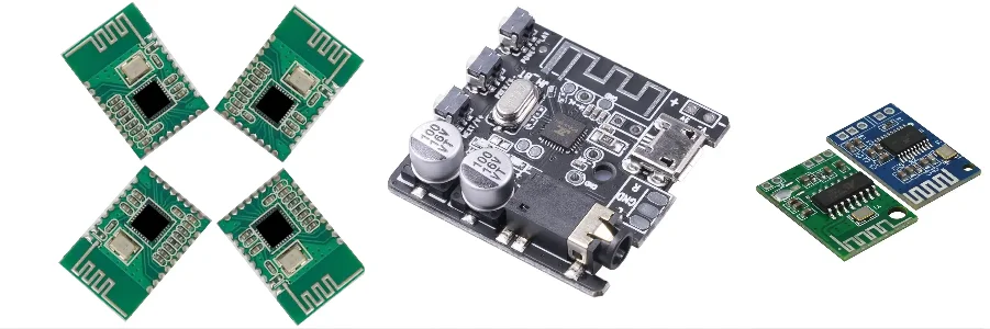
Bluetooth Module Categories:
• Audio Modules: Specialized modules supporting A2DP, HFP, and AVRCP profiles for wireless audio applications with integrated audio codecs and amplifier interfaces
• Data Modules: General-purpose modules supporting SPP, HID, and GATT profiles for sensor data transmission and device control applications
• Combo Modules: Multi-protocol solutions integrating Bluetooth, WiFi, and sometimes cellular connectivity within single packages optimizing cost and board space
• Low Energy Modules: Ultra-low-power modules optimized for IoT sensor applications with extended battery life and mesh networking capabilities
Advanced Assembly Technologies:
HDI PCB construction enables ultra-compact Bluetooth device designs with via-in-pad structures supporting high-density component placement. Sequential lamination processes accommodate complex routing requirements while maintaining excellent RF performance in miniaturized form factors.
Specialized handling procedures for moisture-sensitive Bluetooth modules include controlled storage environments, pre-assembly baking cycles, and assembly within specified timeframes preventing component degradation and ensuring long-term reliability.
Bluetooth Device Applications and Design Optimization
HILPCB delivers Bluetooth PCB manufacturing and assembly solutions for consumer, industrial, medical, and automotive applications, ensuring reliable wireless performance and production-ready quality.
**Consumer Electronics & IoT **
Bluetooth PCBs for audio devices, wearables, and smart home products prioritize low power, compact form factors, and strong RF performance. Flex PCB solutions enable lightweight, space-saving designs ideal for BLE mesh networks and battery-powered devices.
Industrial & Medical Applications
Ruggedized PCBs with enhanced substrates, conformal coating, and regulatory compliance support asset tracking, sensors, and medical devices requiring long-term reliability and data security.
Automotive Systems
Automotive-qualified Bluetooth PCBs meet AEC-Q, EMC, and vibration standards, supporting infotainment, digital keys, and ADAS connectivity with secure, stable wireless communication.
Partnering with HILPCB ensures your Bluetooth devices achieve optimized PCB layouts, regulatory compliance, and scalable manufacturing from prototype to mass production.
Professional Bluetooth PCB Manufacturing & Assembly Services
At HILPCB, we deliver end-to-end Bluetooth PCB manufacturing and assembly solutions, helping you accelerate product development from prototype to high-volume production. Our expertise in high-frequency PCB, fine-pitch assembly, and RF optimization ensures reliable wireless performance and faster time-to-market.
Why Partner with HILPCB:
- Expert RF Design Support – Optimize Bluetooth PCB layouts for range, sensitivity, and EMI compliance using advanced simulation tools.
- Rapid Prototyping & Validation – Quick-turn prototypes with comprehensive RF testing, protocol verification, and certification support.
- Scalable Mass Production – From small batches to millions of units, ensuring consistent quality, on-time delivery, and cost efficiency.
- Full Turnkey Assembly – Component sourcing, precision SMT assembly, programming, functional testing, and secure packaging.
- Comprehensive Quality & Compliance – ISO 9001:2015 certified, RoHS & REACH compliant, with FCC and CE pre-compliance testing to streamline global certification.
With HILPCB as your manufacturing partner, you can shorten development cycles, reduce regulatory risks, and bring high-performance Bluetooth products to market faster.
Frequently Asked Questions About Bluetooth PCB Manufacturing
Q: What are the key considerations for Bluetooth PCB design and manufacturing? A: Bluetooth PCB design requires proper antenna implementation, power management optimization, EMI mitigation, and protocol compliance. Critical factors include substrate selection for 2.4 GHz performance, component placement for RF integrity, and assembly processes ensuring reliable module attachment.
Q: Which materials provide optimal performance for Bluetooth PCB applications? A: Rogers materials offer excellent RF performance for high-end applications requiring maximum range and sensitivity. Quality FR4 substrates work well for cost-sensitive consumer applications. Material selection depends on performance requirements, environmental conditions, and cost targets.
Q: How do you ensure Bluetooth PCB compliance with regulatory requirements? A: We implement comprehensive testing including RF performance verification, spurious emissions measurements, and protocol compliance validation. Pre-compliance testing during design phase minimizes regulatory risks while partnerships with accredited laboratories ensure certification support.
Q: What assembly capabilities do you provide for Bluetooth modules? A: Our services include precision SMT assembly for BGA and QFN packages, specialized reflow profiles for RF modules, moisture-sensitive device handling, and comprehensive testing. We support both prototype quantities and high-volume production with consistent quality standards.
Q: Can you support both Bluetooth Classic and BLE implementations? A: Yes, we provide complete manufacturing and assembly services for all Bluetooth variants including Classic, Low Energy, and advanced Bluetooth 5.x implementations. Our expertise covers audio applications, IoT sensors, and complex multi-protocol designs with appropriate optimization for each application.