
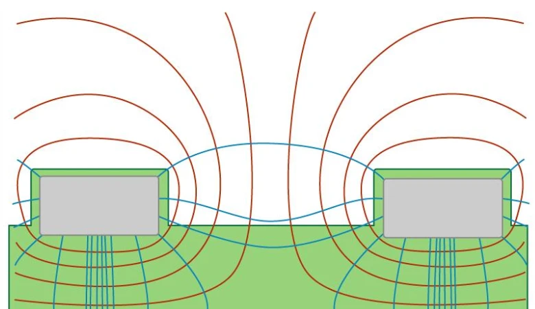
Crosstalk is the unintended transfer of signal energy between adjacent traces—one of the most common signal integrity problems in high-density PCB designs. As signal frequencies increase and trace spacing decreases, crosstalk becomes increasingly significant and must be actively managed.
Understanding crosstalk mechanisms and mitigation strategies is essential for successful high frequency PCB signal integrity.
HILPCB manufactures high frequency PCBs with precise trace geometry control and stackup optimization to minimize crosstalk in demanding applications.
In This Guide
- Understanding Crosstalk
- Capacitive and Inductive Coupling
- Near-End vs Far-End Crosstalk
- Factors Affecting Crosstalk Magnitude
- Measuring and Simulating Crosstalk
- Design Strategies for Crosstalk Reduction
- Crosstalk in Differential Pairs
Understanding Crosstalk
Crosstalk occurs when electromagnetic fields from a switching signal (the "aggressor") couple into an adjacent trace (the "victim"). This coupling adds unwanted noise to the victim signal, potentially causing errors.
Why Crosstalk Matters
Crosstalk degrades signal quality in several ways:
- Reduced noise margin: Added noise makes receivers work harder
- Timing perturbation: Crosstalk pulses shift edge timing
- False triggering: Severe crosstalk can cause logic errors
- EMI concerns: Crosstalk indicates energy transfer that may also radiate
The High-Frequency Challenge
Crosstalk increases with frequency for several reasons:
- Faster edges contain more high-frequency energy
- Coupling mechanisms become more efficient
- Timing margins shrink, making noise more impactful
- Routing density typically increases
A design with acceptable crosstalk at 1 Gbps may have serious problems at 10 Gbps—even with identical geometry.
When Crosstalk Becomes Critical
- High-speed digital (>1 Gbps)
- Dense routing with narrow spacing
- Parallel buses with simultaneous switching
- Sensitive analog/mixed-signal designs
- Long parallel trace runs
- Designs approaching EMC limits
Capacitive and Inductive Coupling
Two distinct mechanisms create crosstalk: capacitive coupling through electric fields and inductive coupling through magnetic fields.
Capacitive Coupling (Cm)
Adjacent traces form a capacitor—changing voltage on one trace induces current in the other. Capacitive coupling:
- Increases with closer spacing
- Increases with longer parallel runs
- Increases with faster edge rates (dV/dt)
- Independent of trace current magnitude
Capacitive coupling creates current flowing in both directions on the victim trace.
Inductive Coupling (Lm)
Current in one trace creates a magnetic field that induces voltage in nearby traces. Inductive coupling:
- Increases with closer spacing
- Increases with longer parallel runs
- Increases with faster current changes (di/dt)
- Proportional to aggressor current
Inductive coupling creates voltage in the same direction as the aggressor signal propagation.
Combined Effect
Real crosstalk combines both mechanisms. The relative contribution depends on geometry and impedance:
- Low-impedance lines: Inductive coupling dominates
- High-impedance lines: Capacitive coupling dominates
- 50Ω typical digital: Both mechanisms contribute similarly
Understanding this helps predict crosstalk behavior and select appropriate mitigation.
Crosstalk Quick Reference
Near-End vs Far-End Crosstalk
Crosstalk manifests differently depending on where you observe it relative to the aggressor signal's travel direction.
Near-End Crosstalk (NEXT)
NEXT appears at the victim's end closest to the aggressor's source—the end the aggressor signal first passes.
Characteristics:
- Combines both coupling mechanisms (they add constructively)
- Pulse width equals aggressor rise time (if coupled region is short)
- Increases with coupled length up to a saturation point
- Saturates when coupled length ≥ (rise time × propagation velocity)/2
- Magnitude relatively independent of coupled length once saturated
NEXT coefficient (Kb): Ratio of backward crosstalk to aggressor amplitude, typically expressed in dB or percentage.
Far-End Crosstalk (FEXT)
FEXT appears at the victim's end farthest from the aggressor's source—the end the aggressor signal approaches.
Characteristics:
- Capacitive and inductive components may partially cancel (depends on geometry)
- Pulse width equals aggressor rise time
- Increases linearly with coupled length (doesn't saturate)
- Can be positive or negative depending on geometry
- In stripline with symmetric geometry, FEXT can be near zero
FEXT coefficient (Kf): Ratio of forward crosstalk to aggressor amplitude.
Practical Implications
- NEXT is often the larger concern for short coupled lengths
- FEXT dominates for long parallel runs
- Stripline naturally reduces FEXT (symmetric field distribution)
- Microstrip typically has larger FEXT than stripline
Factors Affecting Crosstalk Magnitude
Understanding what influences crosstalk guides effective mitigation strategies.
Spacing Between Traces
The strongest factor—crosstalk decreases rapidly with increased spacing.
The 3W Rule: Edge-to-edge spacing equal to 3× trace width reduces crosstalk to approximately 2-3% of the saturated NEXT value. This guideline provides reasonable isolation for many applications.
More aggressive spacing: 5W or greater provides stronger isolation but consumes routing area.
Parallel Run Length (Coupled Length)
- NEXT increases with length until saturation
- FEXT increases linearly without saturation
- Keep parallel runs as short as practical
Height Above Reference Plane
- Closer to reference plane = stronger field confinement
- Stronger confinement = less coupling to adjacent traces
- Thinner dielectric reduces crosstalk
Trace Impedance
- Lower impedance traces have stronger currents, more inductive coupling
- Higher impedance traces have stronger voltage swings, more capacitive coupling
- 50Ω is a balanced compromise
Signal Edge Rate
- Faster edges contain more high-frequency energy
- Coupling efficiency increases at higher frequencies
- Crosstalk increases with faster edge rates
Dielectric Constant
- Higher Dk slows signals, changing coupled length relationship
- Higher Dk may reduce microstrip fringing fields
- Generally minor effect compared to geometry
Measuring and Simulating Crosstalk
Quantifying crosstalk helps verify designs meet requirements.
TDR/TDT Measurement
Time Domain Reflectometry/Transmission can characterize crosstalk:
- Inject fast edge on aggressor
- Measure induced signal on victim (NEXT or FEXT port)
- Results show crosstalk magnitude and timing
VNA S-Parameter Measurement
Vector Network Analyzer provides frequency-domain characterization:
- S21 for FEXT (through measurement)
- S31 for NEXT (coupling measurement)
- Reveals frequency-dependent behavior
- Standard metrics for compliance testing
Simulation Approaches
2D field solvers: Calculate per-unit-length capacitance and inductance matrices. Fast, suitable for uniform coupled lines.
3D field solvers: Handle discontinuities, vias, transitions. More accurate but slower.
SPICE simulation: Use extracted models for time-domain analysis with actual waveforms.
Industry Metrics
Many standards specify crosstalk limits:
- Expressed in dB (S-parameters) or percentage
- Frequency-dependent limits
- Different budgets for NEXT vs FEXT
- Example: 100G Ethernet specifies comprehensive crosstalk masks
Spacing vs Crosstalk Reduction
Design Strategies for Crosstalk Reduction
Multiple approaches reduce crosstalk—often used in combination.
Increase Trace Spacing
The most effective approach when routing density permits:
- Apply 3W rule (or more aggressive) for sensitive signals
- Prioritize spacing for high-frequency and sensitive nets
- Accept tighter spacing for lower-frequency signals
Reduce Coupled Length
Minimize parallel run length between critical signals:
- Route sensitive signals on different layers
- Introduce layer changes to break up parallel runs
- Stagger routing to prevent long parallel segments
Use Ground Shielding
Insert ground traces or copper between aggressors and victims:
- Guard traces: Ground trace between signal traces
- Ground stitching: Vias connecting guard trace to plane
- Coplanar ground: Ground on same layer (CPW structure)
Effectiveness: Guard traces without stitching provide minimal benefit. Vias every ~λ/10 required for effective shielding.
Optimize Stackup
Stackup geometry significantly affects crosstalk:
- Thinner dielectric: Stronger reference plane coupling, less crosstalk
- Stripline: Inherently lower FEXT than microstrip
- Dual stripline: Signals on different layers with ground separation
Route on Different Layers
Signals on different layers with intervening ground plane have greatly reduced crosstalk:
- Orthogonal routing minimizes coupling
- Shared ground plane provides shielding
- Effective for unrelated signal groups
Manage Switching Patterns
Simultaneous switching on adjacent signals creates worst-case crosstalk:
- Spread switching events in time
- Interleave data bits to reduce correlation
- Use differential signaling (common-mode cancellation)
Crosstalk in Differential Pairs
Differential signaling provides inherent crosstalk immunity but introduces additional considerations.
Common-Mode Rejection
Differential receivers reject common-mode noise—crosstalk that appears equally on both traces. This provides significant advantage over single-ended signaling.
However: Crosstalk isn't always perfectly common-mode. Asymmetric coupling creates differential-mode crosstalk that receivers cannot reject.
Pair-to-Pair Crosstalk
Multiple differential pairs in proximity (parallel buses, multi-lane interfaces) experience pair-to-pair crosstalk.
Mitigation:
- Increase pair-to-pair spacing (3W between adjacent pairs)
- Route pairs on different layers
- Insert ground between pairs
- Stagger adjacent pairs to minimize parallel runs
Intra-Pair Crosstalk
The two traces within a differential pair are intentionally coupled. This is desired coupling for differential signaling, not crosstalk.
Design consideration: Maintain consistent coupling (spacing) along the pair for stable differential impedance.
HILPCB Crosstalk-Optimized Manufacturing
HILPCB manufactures high frequency PCBs with the precision required for crosstalk-sensitive designs:
Geometry Control: Precise trace width and spacing for predictable coupling characteristics.
Stackup Optimization: Engineering support for crosstalk-minimizing layer configurations.
Material Options: Range of dielectric thicknesses and Dk values to optimize field confinement.
Testing: S-parameter characterization available for crosstalk-critical designs.
Design Review: DFM analysis includes crosstalk assessment for high-speed designs.
From prototype through volume production, HILPCB delivers consistent crosstalk performance.
Contact HILPCB for high frequency PCB design review and manufacturing quotation.