Ethernet connectivity remains the backbone of modern networking infrastructure, from enterprise data centers to industrial automation systems. As data transmission speeds continue to escalate from Fast Ethernet to multi-gigabit standards, the complexity of Ethernet PCB design has grown exponentially. This comprehensive guide examines the critical aspects of Ethernet PCB design and manufacturing, focusing on the technical challenges that define successful high-speed networking implementations.
The evolution of Ethernet standards has introduced increasingly stringent requirements for PCB layout, signal integrity, and manufacturing precision. Modern Ethernet implementations, particularly those supporting 1000BASE-T, 2.5GBASE-T, and 10GBASE-T standards, demand sophisticated understanding of differential signaling, electromagnetic compatibility, and advanced manufacturing techniques. At HILPCB, our expertise in high-speed PCB manufacturing enables us to address these challenges with precision and reliability.
Ethernet PCB Architecture and System Integration
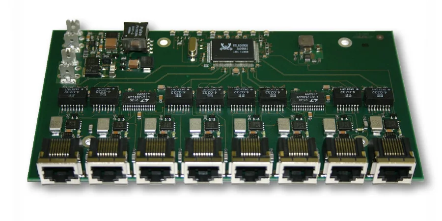
Ethernet PCB architecture fundamentally consists of three interconnected elements: the Media Access Control (MAC) layer, the Physical Layer (PHY) transceiver, and the magnetic isolation circuitry with RJ-45 connectivity. Each component serves a distinct function in the signal processing chain, yet their integration requires careful consideration of electrical characteristics and physical placement.
The MAC layer, typically integrated within microcontrollers or dedicated switching controllers, handles packet formation, collision detection, and media access protocols. Modern implementations often feature integrated MAC/PHY combinations, particularly in microcontroller applications where space optimization is critical. However, high-port-count switching applications frequently require separate PHY transceivers to achieve the necessary channel density and performance characteristics.
Key Architecture Elements:
- MAC/PHY Interface: MII, RMII, GMII, and RGMII protocols with precise timing requirements
- Differential Signaling: 100-ohm impedance control with ±10% tolerance for optimal signal integrity
- Magnetic Isolation: Transformer-coupled circuits with Bob Smith termination for EMI suppression
- Power Management: Multi-rail power delivery with dedicated decoupling strategies
PHY transceivers perform the crucial function of converting digital signals to analog transmission formats suitable for copper or fiber media. These devices implement sophisticated digital signal processing algorithms, including echo cancellation, crosstalk mitigation, and adaptive equalization. The electrical interface between MAC and PHY layers follows standardized protocols, each optimized for specific data rates and implementation requirements.
For applications requiring superior electrical performance, our FR4 PCB solutions provide the foundation for reliable Ethernet implementations while maintaining cost-effectiveness for volume production.
Signal Integrity and Impedance Control for Ethernet PCBs
Signal integrity represents the most critical technical challenge in Ethernet PCB design, particularly for gigabit and multi-gigabit implementations. The fundamental requirement centers on maintaining 100-ohm differential impedance throughout the signal path, from PHY transceiver outputs through magnetic circuits to the RJ-45 connector interface.
Differential impedance control requires precise management of trace geometry, dielectric properties, and electromagnetic field distribution. The relationship between trace width, spacing, and dielectric height determines the characteristic impedance of differential pairs. For typical FR4 constructions with εr = 4.3-4.7, achieving 100-ohm differential impedance typically requires trace widths of 6-8 mils with 6-8 mil spacing on standard stackup configurations.
Critical Signal Integrity Parameters:
- Impedance Control: 100Ω ±10% differential impedance with TDR verification
- Length Matching: Intra-pair skew <50 mils, inter-pair skew <200 picoseconds
- Via Management: Maximum 2 via transitions per trace with controlled pad dimensions
- Return Path Continuity: Uninterrupted reference planes beneath all differential routing
Edge coupling effects between differential trace pairs introduce additional complexity in impedance calculations. When differential traces are spaced closer than 30 mils edge-to-edge, capacitive coupling can reduce the effective differential impedance by 5-20 ohms. This phenomenon necessitates compensation during the design phase through adjusted trace geometry or modified spacing requirements.
Advanced high-frequency PCB materials offer superior electrical performance for demanding Ethernet applications. Low-loss dielectrics with reduced dissipation factors and stable dielectric constants across frequency ranges enable improved signal integrity at multi-gigabit data rates.
Component Placement and Layout Optimization
Strategic component placement forms the foundation of successful Ethernet PCB implementation, directly influencing signal integrity, electromagnetic compatibility, and manufacturing yield. The spatial relationships between PHY transceivers, magnetic circuits, and RJ-45 connectors require careful optimization to achieve optimal electrical performance while maintaining practical manufacturing constraints.
The critical distance between PHY transceivers and magnetic circuits should be maintained at a minimum of 25mm (approximately 1 inch) for EMI mitigation purposes. This separation reduces coupling between high-frequency digital switching noise from the PHY and the sensitive analog circuitry within the magnetic isolation transformers.
Placement Guidelines:
- PHY to Magnetics Distance: Minimum 25mm separation for EMI reduction
- Magnetics to RJ-45 Distance: Maximum 25mm for discrete implementations
- Digital Signal Isolation: 300 mils minimum separation from differential pairs
- Decoupling Placement: Within 10mm of PHY power pins for optimal effectiveness
Differential trace routing between components requires parallel routing with matched lengths and controlled spacing. The total trace length from PHY to connector should not exceed 4 inches (100mm) to minimize signal attenuation and maintain acceptable signal-to-noise ratios. Within this constraint, differential pairs should maintain parallel routing with spacing variations minimized to preserve impedance control and reduce mode conversion.
For complex routing requirements with high pin-count devices, our HDI PCB technology enables compact designs with exceptional routing density while maintaining signal integrity requirements.
Ground Plane Design and EMI Mitigation in Ethernet PCB Manufacturing
Effective ground plane design is critical in Ethernet PCB manufacturing, as it directly impacts signal integrity, EMI suppression, and regulatory compliance. Proper implementation ensures that high‑speed differential signals maintain clean return paths and stable performance.
Key Ground Plane Principles:
- Continuous Reference Planes – Provide uninterrupted ground under all differential traces to maintain low‑impedance return paths.
- Avoid Plane Splits – Gaps beneath differential pairs can disrupt return currents and increase EMI emissions.
- Magnetic Isolation Zones – Keep ground planes clear under discrete magnetic components to prevent unwanted coupling.
- Chassis Ground Integration – Use a dedicated chassis ground for connector modules and EMI shielding.
- Controlled Termination Areas – Maintain proper clearances and impedance around termination regions.
Multi‑layer stackups allow separation of functional grounds while keeping signal layers tightly coupled to adjacent planes, reducing loop inductance and radiated noise. Correct ground plane strategy in Ethernet PCB manufacturing ensures robust EMI performance, signal reliability, and compliance with networking standards.
Professional Ethernet PCB Manufacturing and Assembly Services
At HILPCB, we provide advanced Ethernet PCB manufacturing and assembly services that combine high-frequency design expertise with precision manufacturing capabilities. Our comprehensive approach addresses the complete signal chain from component specifications through final assembly testing, ensuring reliable performance for demanding networking applications.
Manufacturing Capabilities:
- Impedance Control Manufacturing: ±5% tolerance with statistical process control and test coupons
- Advanced Via Technology: Laser-drilled microvias, sequential lamination, and precision plating
- High-Frequency Materials: Rogers substrates and low-loss dielectrics for superior RF performance
- Precision Assembly: 0.4mm BGA placement with ±25µm accuracy and comprehensive AOI/ICT testing
- Quality Systems: ISO 9001:2015 compliance with full traceability and statistical process control
Impedance control manufacturing represents a critical capability for Ethernet PCB production. Achieving the required 100-ohm differential impedance demands precise control of trace geometry, dielectric thickness, and copper plating parameters. Manufacturing process variations in copper plating thickness, dielectric constant, and stack-up registration can significantly impact final impedance values.
Our turnkey assembly services provide complete manufacturing solutions from prototype development through high-volume production, ensuring consistent quality and performance across all production phases.
Testing and validation procedures for Ethernet PCBs encompass both DC electrical characteristics and high-frequency performance parameters. Time-domain reflectometry (TDR) testing validates impedance control and identifies discontinuities in high-speed signal paths. Network analysis characterizes insertion loss, return loss, and crosstalk performance across the frequency ranges relevant to specific Ethernet standards.
Frequently Asked Questions About Ethernet PCB Design
Q: What makes Ethernet PCB design different from standard digital PCBs?
A: Ethernet PCB design requires precise 100-ohm differential impedance control, specialized magnetic isolation circuits, advanced EMI mitigation techniques, and careful component placement to maintain signal integrity at gigabit speeds. The analog nature of the PHY-to-magnetics interface demands superior noise control and return path management.
Q: Which substrate materials are recommended for high-speed Ethernet applications?
A: For 10GBASE-T and higher speeds, low-loss materials like Rogers RO4350B provide optimal performance. Standard high-quality FR4 is suitable for 1000BASE-T applications, while 2.5GBASE-T and 5GBASE-T may benefit from mid-loss substrates depending on implementation requirements and cost constraints.
Q: How do you ensure Ethernet PCB performance meets IEEE standards?
A: We implement comprehensive testing including TDR impedance verification, S-parameter measurements for insertion/return loss, crosstalk analysis, and EMC pre-compliance testing. Our manufacturing processes maintain statistical process control with impedance test coupons and full electrical testing protocols.
Q: What are the critical spacing requirements for Ethernet PCB layout?
A: Key spacing requirements include: PHY to magnetics minimum 25mm separation, magnetics to RJ-45 maximum 25mm for discrete implementations, differential pair to digital signals minimum 300 mils separation, and intra-pair length matching within 50 mils for optimal signal integrity.
Q: Can you support both prototype and production Ethernet PCB requirements?
A: Yes, we provide complete Ethernet PCB services from initial design consultation through high-volume production. Our capabilities include impedance modeling, design optimization, prototype fabrication, precision assembly, comprehensive testing, and ongoing production support with full quality documentation and traceability systems.