
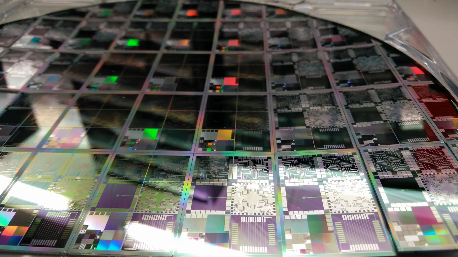
- The first thing to review in HBM3 interposer validation is not one eye diagram or one isolated signoff report, but whether the system budget already places RDL, PI, warpage, assembly, and measurement capability into the same baseline. If different teams stay optimistic in isolation, final signoff becomes distorted very quickly.
- Interposer validation is not simply "DRC passed plus simulation passed." TSMC's public CoWoS-R information states that the RDL interposer can reach
4 μm pitch (2 μm line width/spacing)and uses GSGSG plus interlayer ground shielding to improve signal and power integrity. That means geometry, grounding structure, and process variation directly determine validation difficulty. - PI and SI cannot be signed off separately and then assumed to work together automatically. UCIe 2.0 puts testability, manageability, debug, and telemetry directly into the chiplet and SiP lifecycle, which itself shows that advanced packaging validation has to be organized as a system problem.
- Warpage and CTE mismatch are not back-end assembly issues. They are main variables inside interposer validation itself. TSMC also publicly states that CoWoS-R uses RDL layers and C4/underfill layers to buffer CTE mismatch between SoC and substrate and reduce strain energy density around the C4 bump region. That means mechanical behavior is already inside the electrical window.
- A truly valuable release criterion is not that the final product "worked once," but that the same behavior can be repeatedly explained across test vehicles, engineering samples, and low-volume pilot builds.
Quick Answer
The core of HBM3 interposer validation is not just one round of SI or PI signoff. It is aligning system budget, RDL process window, warpage behavior, assembly conditions, and test vehicles under one shared set of assumptions. In 2.5D and advanced packaging programs, the earlier models are aligned with physical hardware, the less rework shows up during pilot manufacturing.
Table of Contents
- What should engineers review first in HBM3 interposer validation?
- Summary table of key rules and parameters
- Why must validation begin with system-budget decomposition?
- Why can't RDL density be checked only against nominal design rules?
- Why must PI, SI, and warpage be validated together?
- Why do test vehicles create value earlier than final signoff?
- Next steps with HILPCB
- Frequently Asked Questions (FAQ)
- Public references
- Author and review information
What should engineers review first in HBM3 interposer validation?
Start with system budget, the RDL process window, PI/SI interaction, warpage behavior, test vehicles, and the measurement path.
This does not mean "run the channel simulation first and fill in the rest later," and it does not mean "one package signoff proves the interposer is mature." JEDEC publicly treats HBM as one of the main memory technology focus areas. UCIe 2.0 brings manageability, debug, testing, and telemetry into the multi-chip SiP lifecycle. The SEMI APHI community places manufacturing readiness directly into the mission of advanced packaging. Put together, the clearest conclusion is that HBM3 interposer validation is a system-engineering task before it is a single-point simulation task.
Before design freeze, the five questions that are usually most useful are:
- Do loss, skew, PI droop, warpage, and assembly all consume one shared budget?
- Where are the densest RDL regions, the most sensitive regions, and the most fragile regions?
- Are PI, SI, and mechanical models describing the same geometry?
- Do the test vehicles really map the true bottlenecks instead of only ideal channels?
- During pilot build, can anomalies be measured, explained, and traced back to physical location?
If the project is still comparing dense-interconnect paths against manufacturing window, it is usually worth bringing the geometric and validation logic of HDI PCB and High-Speed PCB into the review early as analogies, instead of treating advanced packaging as a special world disconnected from manufacturing discipline.
Summary table of key rules and parameters
| Rule / Parameter | Recommended range or judgment method | Why it matters | How to verify | What happens if ignored |
|---|---|---|---|---|
| System budget | Put loss, skew, PI, warpage, and assembly into one common baseline | Every team is spending the same shared margin | Budget review, cross-functional review | Each signoff passes locally while the total system stays unstable |
| RDL process window | Check line width, spacing, dielectric, and grounding variation beyond nominal values | Interposer behavior is highly sensitive to geometry | Corner simulation, cross-section, CD data | Nominal looks safe, corners go unstable |
| PI/SI interaction | Review return paths, droop, and crosstalk inside the same model | Simultaneous switching and bump congestion couple together | Co-simulation, representative channel sampling | Separate conclusions conflict with each other |
| Warpage and CTE | Manage deformation separately across assembly temperature and thermal cycling | Mechanical movement rewrites electrical behavior | Warpage measurement, before/after thermal cycle comparison | Electrical anomalies get misdiagnosed long term |
| Test vehicle | Build the weakest structure first, not only the easiest one to measure | The earlier model and hardware align, the lower the cost | Vehicle test, back-annotation, failure analysis | Risk gets delayed to the final product |
| Measurement traceability | Every anomalous lane, region, and process revision must be bindable | Advanced packaging suffers most when anomalies are visible but not explainable | Revision control, mapping, FA path | Pilot anomalies do not converge |
| Public basis | Direct implication for validation |
|---|---|
| TSMC CoWoS-R: minimum 4 μm pitch, GSGSG, interlayer shielding | RDL geometry and grounding structure are validation variables by themselves |
| TSMC CoWoS-R: RDL plus C4/UF buffer CTE mismatch | Warpage and assembly are not optional later-stage topics |
| UCIe 2.0: DFx, testing, telemetry, manageability enter the lifecycle | Advanced packaging has to be organized around system-level validation |
| SEMI APHI: manufacturing readiness is a core goal | Validation should not stop at models; it should move toward manufacturing readiness |
Why must validation begin with system-budget decomposition?
Conclusion: Because loss, skew, droop, warpage, and assembly behavior on an HBM3 interposer all consume the same system margin together.
UCIe 2.0 directly brings testability, manageability, debug, and telemetry into the chiplet and SiP lifecycle. That is not just a management layer addition. It is an explicit warning that advanced packaging validation becomes fragmented if it does not begin from one shared system budget.
What is worth freezing first includes:
- Channel-loss and crosstalk budget
- Byte-lane and channel skew budget
- PDN droop and transient budget
- Warpage budget across assembly temperature and thermal cycling
- Measurement resolution and anomaly-localization budget
If these budgets are not tied to the same geometry and process assumptions, later SI, PI, and assembly validation often becomes a case where "every team is right on its own, but the system still does not fit together."
Why can't RDL density be checked only against nominal design rules?
Conclusion: Because at HBM3-class interconnect density, variation in RDL geometry itself is enough to rewrite signal, power, and assembly behavior.
TSMC's CoWoS-R page gives several key public facts: the RDL interposer can reach 4 μm pitch (2 μm line width/spacing), coplanar GSGSG and interlayer ground shielding are used to improve signal and power integrity, and the RDL plus C4/underfill layers help buffer CTE mismatch between SoC and substrate. For validation, all of that means geometry, shielding, and mechanical buffering are not separate topics.
What deserves early confirmation includes:
- Where the densest RDL regions are
- Which areas are most sensitive to line width, spacing, dielectric, and copper-profile variation
- Whether local shielding and return structures still hold at process corners
- Whether the process-corner model still keeps the window after nominal DRC passes
If the project is still comparing dense-interconnect and structural windows, it is usually helpful to reference the manufacturing logic of HDI PCB and reason backward from manufacturable fragility instead of reading only nominal layout results.
Why must PI, SI, and warpage be validated together?
Conclusion: Because electrical behavior and mechanical behavior on an HBM3 interposer are not two systems. They are one coupled system.
When return-path changes, bump congestion, local reference variation, and simultaneous switching all occur together, SI results are directly shaped by PI and mechanical deformation. And once TSMC publicly includes CTE-mismatch buffering inside CoWoS-R features, it becomes even clearer that warpage and underfill/C4 behavior cannot be left as a separate downstream assembly topic.
What is worth checking together includes:
- Insertion loss, return loss, and crosstalk on representative channels
- Local droop and resonance on the same structure
- Warpage change before and after thermal cycling and reflow
- Whether bump/underfill-sensitive areas overlap critical channels or critical power regions
If the current task is mainly evaluating coupling between high-speed interconnect and power integrity, it is useful to treat the return-path logic of High-Speed PCB and the power/reference organization of Multilayer PCB as baseline analogies, then tighten the assumptions for advanced packaging instead of splitting PI and SI completely apart.
Why do test vehicles create value earlier than final signoff?
Conclusion: Because test vehicles expose the most dangerous mismatch between model, process, and measurement before the final product is frozen.
SEMI APHI places manufacturing readiness directly into the mission of advanced packaging. That means validation should not stop at "the simulation file passed." It should push toward "manufacturable, measurable, and traceable." For an HBM3 interposer, that is exactly the role of a test vehicle.
The most valuable test vehicles usually cover:
- The densest RDL zones and the most fragile transition zones
- Return and shielding structures that distort most easily
- Hotspot regions most related to warpage and CTE
- Alignment marks and inspection points that map into measurement and failure analysis
If the project is close to engineering samples or pilot build, it is often better to fold the vehicle plan into the engineering inputs for PCB Prototype and Quote / RFQ rather than delaying the exposure of risk until the final product stage.
Next steps with HILPCB
If you are currently working on HBM3 interposer validation, 2.5D/3D advanced-packaging support validation, or a dense chiplet-interconnect project, the next step is usually to turn "simulation passed" into "the structure is close to manufacturing and measurement reality."
- When the main issue is dense interconnect geometry plus return/shielding structure, first compare the geometry and validation logic of HDI PCB and High-Speed PCB.
- When the project is still comparing power/reference organization and local density windows, include the stackup perspective of Multilayer PCB in the same review.
- When the most fragile structures, densest zones, and test-vehicle logic need early validation, moving those checks into PCB Prototype exposes problems earlier.
- Once the validation matrix, measurement path, and anomaly traceability are frozen, organizing them into Quote / RFQ improves later engineering communication.
Frequently Asked Questions (FAQ)
Is looking at SI first enough for HBM3 interposer validation?
A: No. SI is only one part of the result. RDL variation, PI, warpage, and assembly window all rewrite the final margin together.
If all nominal design rules pass, why might the design still be unsafe?
A: Because advanced-packaging geometry is extremely sensitive. Small variation under process corners or assembly corners can turn nominally safe into corner-unstable.
Why must warpage be reviewed together with electrical validation?
A: Because coplanarity, CTE mismatch, and underfill/bump behavior directly change contact condition and local return paths, and that eventually appears as electrical anomalies.
Why are test vehicles so important?
A: Because they align model, process, and measurement earlier, instead of delaying the largest risk until the final product stage.
What is most worth freezing before sample build or pilot production?
A: Prioritize system budget, RDL process window, PI/SI interaction assumptions, warpage path, test-vehicle plan, and measurement traceability method.
Public references
JEDEC Home
Supports the article's context that HBM is part of JEDEC's main memory technology focus and should be understood inside a formal standards ecosystem.UCIe Specifications
Supports the article's explanation that UCIe 2.0 brings testability, manageability, debug, telemetry, and 3D packaging into the multi-chip SiP lifecycle.TSMC CoWoS® Technology
Supports the article's explanation that CoWoS-R uses an RDL interposer between SoC and HBM, can reach 4 μm pitch, uses GSGSG/interlayer shielding, and uses RDL plus C4/underfill to buffer CTE mismatch.SEMI APHI Technology Community
Supports the article's explanation that SEMI treats manufacturing readiness, technology gaps, proof-of-concept, and standards as core advanced-packaging goals.
Author and review information
- Author: HILPCB High-Density Interconnect and Advanced Packaging Content Team
- Technical review: SI, PI, reliability, and process engineering team
- Last updated: 2026-05-18