

Modern RF and high-speed systems—5G base stations, automotive radar, satellite terminals and data center switches—are all built on high-frequency PCB platforms. In these products, the PCB is not just a mechanical carrier: it is a key RF, microwave and signal-integrity component that defines loss, phase, beam steering and channel margin.
This article looks at high-frequency boards from a system point of view: what a 5G base station PCB manufacturer, mmWave radar PCB manufacturer, satellite communication PCB production partner or high-frequency data center PCB supplier actually needs to control, and how HILPCB supports those requirements from design through volume manufacturing.
To keep the structure clear and useful, the guide is organised into five sections:
- [1. Where High-Frequency PCBs Fit in 5G, Radar, Satellite and Data Centers]
- [2. Electrical and Mechanical Requirements by Application Segment]
- [3. RF Front-End Module and Microwave PCB Engineering]
- [4. From Prototype to Volume: Industrialising Complex HF PCB Platforms]
- [5. Reliability, Safety and Long-Term Platform Strategy]
1. Where High-Frequency PCBs Fit in 5G, Radar, Satellite and Data Centers
High-frequency PCBs sit at the centre of combined RF, mixed-signal and high-speed digital architectures. Each sector uses them differently, but the underlying need is the same: predictable electrical behaviour over time and volume.
1.1 5G base stations and wireless access networks
For radio access networks, a 5G base station PCB manufacturer supports:
- Distributed RF tiles and massive MIMO arrays with tight phase and gain consistency
- Split architectures (RF, IF and baseband on separate but coordinated boards)
- High duty cycles in outdoor environments with demanding thermal and mechanical constraints
In this context, wireless communication equipment PCB manufacturing must deliver stackups and routing rules that keep isolation, loss and linearity inside specification across many carriers and bands.
1.2 Automotive radar and autonomous driving systems
Automotive radar PCB design is part of wider autonomous driving PCB solutions that also include:
- Multiple radar units with overlapping coverage and redundancy
- High-performance computing platforms for sensor fusion and perception
- Vehicle-level EMC, thermal and mechanical requirements
Here, a mmWave radar PCB manufacturer has to treat the board as a precise 77–79 GHz RF structure and as an automotive electronics platform at the same time, especially where long lifetime and functional safety are involved.
1.3 Satellite communication hardware
Satellite communication PCB production covers:
- Space payload electronics and RF front ends
- Ground gateways and user terminals
- Tracking, telemetry and control subsystems
These boards must combine low-loss RF performance with extreme reliability under thermal cycling, radiation and long mission durations. The PCB is a critical part of both the RF chain and the mechanical structure.
1.4 High-speed data center infrastructure
High-frequency data center PCB platforms support:
- High-speed serial links on backplanes, line cards and interconnect modules
- Tight loss and skew budgets over long PCB channels
- Coexistence of extremely hot ASICs and dense power delivery networks with fragile high-speed differential pairs
Although the signals are digital, the design philosophy is close to RF engineering: channel loss, impedance and crosstalk define what throughput is achievable.
2. Electrical and Mechanical Requirements by Application Segment
Different applications share common concepts—controlled impedance, low loss, thermal management—but they apply them in different ways. Treating all high-frequency boards as identical often leads to over- or under-specification.
2.1 5G base stations and wireless communication equipment
For a 5G base station PCB manufacturer and wireless communication equipment PCB manufacturing partner, key requirements include:
- Multi-band RF performance Stackups that support multiple bands with controlled impedance and stable loss, including clean separation between bands and between RF and digital sections.
- Isolation and coexistence Layer planning, via fences and cavity structures to achieve isolation between power amplifiers, LNAs, LO distribution and baseband processing.
- Thermal and mechanical robustness Copper distribution, thermal vias and mechanical constraints that maintain PA efficiency and LNA noise performance while surviving outdoor thermal cycling.
These factors influence material choices, geometry limits and panelisation strategies for radio and backhaul boards.
2.2 Automotive and industrial radar platforms
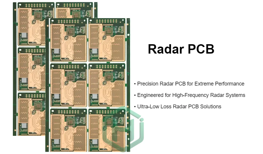
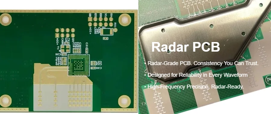
For automotive radar PCB design and mmWave radar PCB manufacturers, the constraints tighten:
- Short wavelength sensitivity At tens of GHz, every via, pad and discontinuity affects beam patterns and sidelobe levels; layout errors cannot be “fixed” in software.
- Integrated antennas and RF feed structures Antennas, feed networks, power dividers and couplers are often implemented directly in copper and dielectric, rather than as external components.
- Automotive environment and safety Operation over wide temperature ranges, under vibration and contaminants, while meeting functional safety standards and lifetime expectations.
In a broader autonomous driving PCB solutions context, these radar PCBs must interface cleanly with sensor fusion processors, power stages and vehicle networks.
2.3 Satellite communication and ground segment boards
Satellite communication PCB production focuses on:
- Tightly controlled loss and phase Long RF paths and feed networks require low-loss laminates, stable Dk and carefully controlled geometries.
- Qualified materials and traceability Strict control of laminates, copper, finishes and process histories for certification and long-term support.
- Mechanical and thermal integrity Stackups and mounting concepts that withstand launch loads (for in-orbit equipment) and environmental extremes in ground stations.
These conditions mean that reliability and documentation are as critical as raw RF performance.
2.4 High-frequency data center PCBs
For high-frequency data center PCB platforms, requirements include:
- Channel engineering and modelling Well-defined insertion loss, return loss and crosstalk across long, complex routes, grounded in accurate material and geometry data.
- Material and stackup selection Using low-loss dielectrics in critical channel regions, while balancing cost and manufacturability for large-format backplanes and high-layer-count line cards.
- Thermal and power integrity Routing and copper planning that support high-current power delivery and effective cooling without compromising signal integrity.
Here, PCB constraints often define whether a new generation of network gear can reach its target interface speeds at acceptable power levels.
3. RF Front-End Module and Microwave PCB Engineering
A large fraction of high-frequency systems are built from compact blocks based on RF front-end module PCB designs and microwave assemblies. Choosing where and how to buy microwave RF PCBs is therefore a strategic decision.
3.1 RF front-end module PCB requirements
RF front-end module PCB platforms for 5G, Wi-Fi, IoT and radar chains must provide:
- Controlled transitions between die, packages and board Via-in-pad design, pad geometries and launch structures tuned to minimise parasitics and resonances at the operating band.
- Embedded passives and matching networks Filters, couplers, baluns and matching networks realised in copper and dielectric to save space and reduce interconnect loss.
- Clean biasing and power distribution Bias lines, decoupling networks and returns arranged to avoid injecting noise into sensitive RF nodes.
A manufacturing partner experienced in RF front-end module PCB work can reduce iteration count and improve correlation between EM simulation and lab measurements.
3.2 Microwave and phased array radar boards
For microwave links and phased arrays, a phased array radar PCB supplier must support:
- Array-level phase and amplitude control Consistent line lengths, impedances and material properties across large panels and many elements.
- Complex multilayer RF structures Multi-level feed networks, couplers and power dividers distributed across several carefully designed layers.
- Mixed-signal coexistence RF layers sharing the stackup with timing and control logic, requiring disciplined reference-plane and isolation strategies.
In this context, the PCB behaves as part of the beamforming network, not just as a carrier for ICs and connectors.
3.3 Sourcing microwave and RF PCBs with the right capabilities
When engineers ask where to buy microwave RF PCBs, they usually need more than fine-line capability. Practical criteria include:
- Proven RF stackups and materials for the relevant frequency and environment
- Stable, characterised process windows for critical RF geometries and transitions
- Integrated fabrication and assembly flows, including handling of delicate RF, mmWave and mixed-signal components
HILPCB structures its microwave and RF services around these expectations, so module designers can move from breadboards to manufacturable RF front-end module PCB platforms without changing suppliers.
4. From Prototype to Volume: Industrialising Complex HF PCB Platforms
For all of these applications—5G, radar, satellite and data center—the hardest part is not the first working board. It is turning that board into a robust, repeatable platform that supports multiple product generations.
4.1 Prototyping and early system integration
In early stages, design teams focus on:
- Architecture and partitioning Exploring how to split functionality between RF, mixed-signal and digital boards, and where to place critical components.
- Rapid PCB and assembly iteration Short cycle times for layout changes and small-batch builds, allowing quick feedback from the lab to the CAD tool.
- Measurement-driven refinement Using S-parameters, eye diagrams, beam patterns and thermal measurements to refine stackups, materials and routing rules.
At this stage, a flexible manufacturing partner that understands high-frequency constraints is more valuable than a vendor optimised only for volume.
4.2 Transition to controlled, recurring production
As designs stabilise, industrialisation requires:
- Defined stackups and design rules Documented materials, layer arrangements and geometry rules tailored to each application segment.
- Process capability and variability control Monitoring critical dimensions and electrical parameters across production lots to ensure performance stays inside a defined window.
- Assembly and test integration Aligning stencil designs, reflow profiles and test strategies with PCB design choices to protect RF and high-speed performance.
For satellite communication PCB production this includes tight configuration management and traceability; for high-frequency data center PCBs it means tracking evolving interface standards and updating stackups without destabilising existing products.
4.3 Adapting to different volume and lifecycle profiles
Different markets behave very differently:
- 5G radios may ramp quickly and then evolve through several hardware generations.
- Automotive radar and autonomous driving PCB solutions require long production lifetimes and tightly controlled design changes.
- Satellite and specialised microwave products may be built in modest volumes but demand extended support and requalification discipline.
A strong manufacturing partner adjusts planning, capacity and documentation to each of these profiles while keeping the underlying PCB platforms electrically consistent.
5. Reliability, Safety and Long-Term Platform Strategy
In infrastructure and mission-critical systems, high-frequency PCBs are long-lived assets. Reliability, safety and roadmap alignment are as important as the first lab measurement.
5.1 Reliability and safety in demanding environments
A robust 5G base station PCB manufacturer, mmWave radar PCB manufacturer or satellite communication PCB production partner must focus on:
- Material and finish stability over time Ensuring that dielectric properties, copper behaviour and interface finishes remain within specification under real operating conditions.
- Interconnect and via robustness Designing via structures and aspect ratios to survive thermal cycling, mechanical stress and repeated assembly operations.
- Safety-driven design choices Supporting redundancy, diagnostics and safe-fail behaviour in automotive radar PCB design and autonomous driving PCB solutions.
These choices reduce field failures, warranty costs and safety risks across the entire product fleet.
5.2 Lifecycle support, diagnostics and upgrade paths
Long-lived systems need thoughtful lifecycle engineering:
- Serviceability Boards and modules designed with clear diagnostic access and replacement strategies, supported by reference test data and documentation.
- Upgrade capability PCB platforms that can absorb new bands, additional radar channels or higher data rates without complete redesign, especially in wireless networks and high-frequency data center PCB environments.
- Feedback loops into new designs Using field and test data to improve future revisions and related product families instead of treating each design as an isolated project.
This approach aligns high-frequency PCB platforms with long-term network and system roadmaps.
5.3 Building long-term platforms with a trusted HF PCB partner
Ultimately, the most valuable relationship is not a one-off board order but a long-term collaboration. For 5G radios, radar systems, satellite communication hardware and data center equipment, this means:
- A consistent set of high-frequency PCB design rules and stackups, refined over time
- A clear view of process capabilities and limits shared between design and manufacturing teams
- Joint planning for future performance, integration and cost targets
HILPCB positions its high-frequency PCB platforms to support exactly this kind of long-term system strategy. Whether you are building RF front-end module PCB families, automotive radar units, satellite terminals or high-frequency data center PCBs, our goal is to provide a stable, predictable PCB foundation that you can build on for multiple generations of products—not just a single release.
Common Questions
Why do radar, satellite, and 5G systems place such high demands on high-frequency PCB platforms?
Because these systems care about more than basic connectivity. Loss, phase consistency, beam control, and long-term stability all depend on the PCB, so the board becomes part of the electrical platform itself.
What is hardest to control when multiple RF applications share a common platform?
Balancing materials, stackup rules, assembly tolerance, and different application constraints is usually the hardest part. Platforming is not just reusing one template; it means building a controlled foundation that still protects critical performance.
Why is long-term platform strategy so important in this category?
Because the expensive part is rarely building one working prototype. The real cost comes when each next-generation product repeats the same material, process, and performance mistakes instead of inheriting a stable platform.