
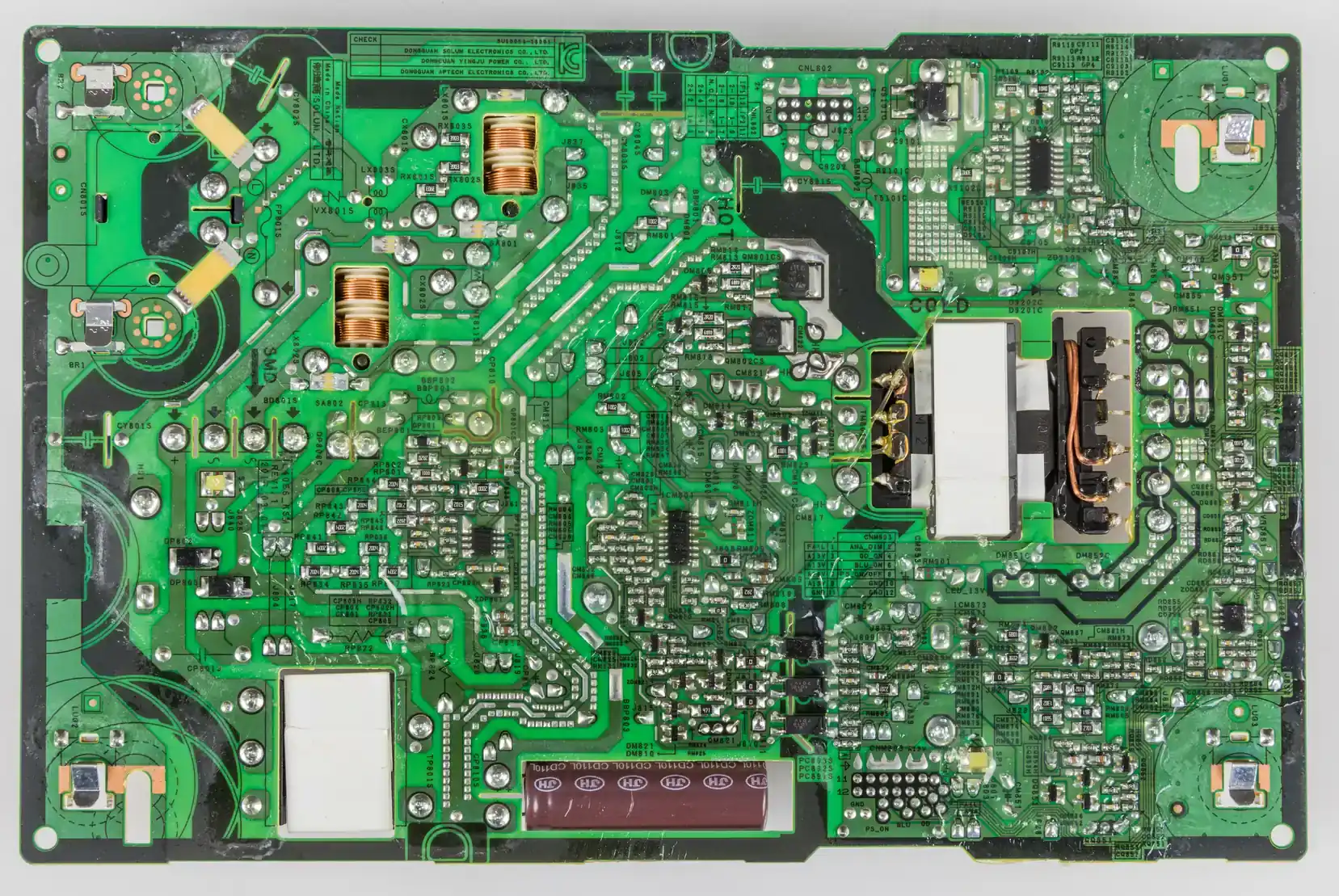
An LCD power supply PCB is not just a board that turns input voltage into panel power. In a modern display product, it may support LED or Mini-LED backlight rails, panel logic, T-CON supply, source and gate driver rails, touch sensing power, interface protection, dimming control, standby power and system telemetry. If the board is noisy, thermally overloaded or difficult to test, the failure may appear as flicker, rolling bands, false touch events, brightness instability, audible noise, EMI failure or premature field returns.
For HILPCB, the useful engineering question is not whether an LCD power supply board resembles a data center server PCB. The better question is: which display loads must be powered, which rails are noise-sensitive, which switching loops are high-current, and which production checks are needed before the design is released?
Key takeaways
- LCD display power is a mixed-signal power problem: high-current LED backlight rails coexist with sensitive timing, touch and interface circuits.
- Mini-LED local dimming increases power-channel count, transient current demand, layout density and thermal stress.
- Ripple, switching noise and poor return-path planning can become visible artifacts on the screen or false triggers on touch circuits.
- Heavy copper, thermal vias, metal-core structures and high-thermal materials are useful only when they match the real heat path and enclosure design.
- PCB manufacturing can support IEC 62368-1, ENERGY STAR, VESA DisplayHDR and interface-level validation, but a PCB alone does not prove product safety, efficiency, HDR performance or system compliance.
In this guide
- What an LCD power supply PCB actually powers
- Power integrity for display quality
- Backlight and Mini-LED driver PCB design
- Thermal design for compact display electronics
- EMI, grounding and interface protection
- Touch, 3D touch, VR and advanced display subsystems
- Safety, efficiency and display-performance boundaries
- Manufacturing, PCBA testing and reliability controls
- Common failure modes
- Cost drivers
- RFQ checklist
- FAQ
What an LCD power supply PCB actually powers
An LCD module typically contains more than one power domain. The exact rail count depends on the panel, backlight architecture, touch stack and product category, but the same board-level questions appear again and again.
The backlight power section usually handles the largest current. For edge-lit LED displays, this may be one or more constant-current LED channels. For direct-lit or Mini-LED backlights, the channel count can increase dramatically because the system needs multiple dimming zones. This section normally uses switching converters, MOSFETs, inductors, current-sense circuits and protection devices. It is the strongest source of heat and EMI on many LCD power boards.
The panel logic and T-CON rails are lower-current but more noise-sensitive. Timing controllers, source drivers and gate-driver power circuits need stable supplies because noise or droop can disturb grayscale accuracy, scan timing or driver behavior. A board that passes a basic power-on test may still fail under motion scenes, high brightness or cold start if these rails are not validated under realistic display patterns.
The touch and sensing rails require even cleaner separation. Capacitive touch, 3D touch, ambient-light sensing and proximity sensing can be affected by switching ripple, ground bounce and display refresh noise. A power board for a touch display must not treat the sensing section as a simple low-current accessory. It needs intentional filtering, return-path control and placement discipline.
The interface and control section may include eDP, LVDS, MIPI, HDMI, DisplayPort-related protection, I²C, SPI, UART, USB, GPIO, backlight PWM, local dimming data and fault telemetry. These are not always routed on the power board itself, but their references, connectors and ESD protection often are. Poor grounding near these connectors can convert a power-board problem into a system-level display or communication failure.
A practical review begins by classifying the board into one of these routes:
| Board route | Typical display application | Dominant PCB concern | HILPCB manufacturing focus |
|---|---|---|---|
| Basic LCD power board | Industrial display, monitor, signage, HMI | Stable panel rails and LED backlight conversion | Multilayer layout, controlled soldering, power test |
| High-brightness backlight board | Outdoor signage, medical display, HDR monitor | High current, heat spreading, EMI | Heavy copper, thermal vias, functional load test |
| Mini-LED driver board | HDR monitor, premium TV, display wall | Multi-channel current matching and dense routing | HDI, fine-pitch SMT, AOI and FCT |
| Touch display power/control board | POS, kiosk, tablet, HMI | Noise isolation for capacitive sensing | Mixed-signal layout review, filtering, ESD protection |
| Tethered VR or near-eye display board | VR headset, simulation display, wearable terminal | Size, heat, high-speed interfaces, user comfort | Rigid-flex, HDI, lightweight PCBA assembly |
| Laser or projection light-source board | Projector, optical engine, industrial display | Current control, safety interlocks, thermal paths | High-thermal PCB, inspection, traceability |
The board should not be described as a universal “display PCB” until this route is clear. A small TFT control board, a Mini-LED backlight driver, a VR headset display module and a laser-light-source board may all belong to display technology, but they create different manufacturing risks.
Power integrity for display quality
Power integrity decides whether each rail stays within its useful operating window during real display behavior. A static bench load is not enough. Displays change current demand with brightness, refresh rate, local dimming, touch interaction, input mode and thermal state.
For LCD power supply PCBs, the most visible power integrity problems usually come from three sources.
First, switching ripple can couple into panel logic or analog sensing. Ripple from boost, buck or buck-boost regulators may appear as flicker, faint bands, brightness pumping or unstable grayscale behavior. The layout around switching nodes, input capacitors, current-sense loops and feedback traces often matters as much as converter selection.
Second, transient response becomes harder when brightness changes quickly. HDR scenes, local dimming algorithms and high refresh rates can cause rapid load steps. The PCB must support low-inductance current paths, suitable bulk and high-frequency decoupling, and stable feedback routing. If the rail droops during a bright scene, the user may see backlight instability even if the schematic looks correct.
Third, ground bounce and return-path errors can corrupt low-level circuits. The display power section may share connectors, cables or planes with touch, T-CON and communication circuits. If return currents are not planned, high-current pulses can move the local reference for sensitive circuits.
Display power rails and review points
| Power rail or function | Common load | Main PCB risk | Review action |
|---|---|---|---|
| LED backlight boost rail | LED strings or Mini-LED zones | Switching noise, high current, MOSFET heating | Minimize hot loop area and define thermal path |
| Constant-current channel | LED driver outputs | Channel mismatch, sense noise, connector heating | Route current sense carefully and test under brightness patterns |
| Panel logic rail | T-CON and control logic | Ripple-induced timing instability | Provide clean decoupling and stable return plane |
| Gate/source driver rails | LCD driver ICs | Overshoot, start-up sequencing, noise | Validate startup and shutdown sequence with panel attached |
| Touch controller rail | Capacitive sensing front end | False touch from power noise | Use filtering, segmentation and quiet ground reference |
| Interface protection | HDMI, USB-C, eDP, LVDS or MIPI interface area | ESD return injection and common-mode noise | Place TVS devices near connector and protect return path |
| Standby rail | MCU, remote control, wake circuit | Efficiency and leakage | Verify sleep-mode power with final firmware |
A strong LCD power supply PCB review connects these rails to real tests: ripple under full brightness, dimming pattern transitions, cold start, hot enclosure operation, standby mode, touch interaction and cable ESD scenarios.
Backlight and Mini-LED driver PCB design
The backlight section is where display power boards often become difficult. It is also where overgeneralization is common. A simple edge-lit LCD monitor and a high-zone-count Mini-LED display do not need the same board strategy.
A conventional LED backlight driver usually needs a stable current source, fault detection and efficient voltage conversion. The design focus is hot-loop control, inductor placement, current-sense integrity, LED connector robustness and thermal spreading.
A Mini-LED backlight board adds more complexity. Local dimming requires multiple current channels, tighter channel-to-channel matching and faster control response. The PCB may need more driver ICs, more current-sense traces, more connectors, more copper area and more test coverage. The power board becomes part of the image-quality chain rather than a passive supply.
Backlight driver layout rules that matter
- Keep switching loops short and local. The loop from input capacitor to MOSFET, diode or synchronous switch and inductor must be compact. Long loops raise EMI and ringing.
- Protect current-sense nodes. Sense traces should not run beside switching nodes, LED output cables or high-current copper pours unless shielding and spacing are planned.
- Treat LED connectors as power and EMI components. Connector pinout, creepage, current rating, strain relief and return arrangement affect both reliability and emissions.
- Design for real dimming patterns. Full-white steady state is not the only load case. Checkerboard, low-duty PWM, local-dimming transitions and high-brightness highlight windows can stress the supply differently.
- Avoid thermal crowding. Driver ICs, inductors, MOSFETs, sense resistors and connectors should not be packed into one small hot island unless the enclosure heat path is already defined.
Backlight architecture comparison
| Backlight type | PCB complexity | Power-design concern | Testing priority |
|---|---|---|---|
| Edge-lit LED | Low to medium | Efficient constant-current drive and connector reliability | Ripple, current accuracy, thermal rise |
| Direct-lit LED | Medium | Multi-string balancing and heat spreading | Channel balance, LED fault detection |
| Mini-LED local dimming | High | Many current channels, fast transient response, dense routing | Dimming-pattern stress, EMI, thermal imaging |
| High-brightness outdoor LCD | High | High current, heat, surge and environmental protection | Full-brightness burn-in, thermal and surge checks |
| VR / near-eye backlight | Medium to high | Low noise, low heat, compactness, cable routing | User-temperature limits, flicker and interface stability |
For production, backlight test coverage should include current accuracy, open/short LED detection, PWM or digital dimming behavior, fault reporting, thermal rise and connector temperature under realistic operating modes.
Thermal design for compact display electronics
Thermal design is not only about preventing immediate overheating. In display power electronics, thermal drift can change current sensing, reduce capacitor life, increase LED color/brightness variation and accelerate solder-joint fatigue. Compact enclosures and thin bezels make this worse because airflow is limited.
The PCB heat path begins at the component. MOSFETs, Schottky diodes, synchronous rectifiers, inductors, LED drivers, current-sense resistors and protection components should be placed with their thermal paths in mind. If the enclosure will clamp to the board, the board needs defined contact zones and controlled keepouts. If the board depends on airflow, the layout should avoid blocking hot components behind tall connectors or shields.
PCB thermal options
| Thermal method | Where it helps | Engineering caution |
|---|---|---|
| Large copper pours | LED current paths, MOSFET drains, driver IC heat spreading | Copper balance and solderability must be controlled |
| Thermal via arrays | QFN, power ICs, LED drivers, hot regulators | Via fill, solder wicking and assembly process must be reviewed |
| Heavy copper PCB | High-current backlight and power-distribution areas | Increases etching, lamination and fine-pitch routing difficulty |
| Metal core PCB | High-power LED backlight or laser-light-source boards | Electrical isolation and assembly process windows must be verified |
| High-thermal substrate | Compact power boards with limited airflow | Must match soldering, mechanical and cost targets |
| Thermal interface material | Board-to-chassis or component-to-housing path | Compression, aging and reworkability should be specified |
For HILPCB, the practical review question is: where does heat leave the board? If the answer is not tied to copper, vias, mechanical contact, enclosure material and load test, the thermal design is not yet complete.
EMI, grounding and interface protection
LCD power supply PCBs generate EMI because they switch current rapidly. The risk grows when the board includes long LED cables, high-current connectors, metal enclosures, touch sensors or high-speed display interfaces.
The first EMI rule is to control the source. Hot loops must be compact, switching nodes should be kept away from connectors and sensitive traces, and snubber or damping footprints should be reserved if the converter needs tuning. Gate-drive resistor footprints and current-sense filtering options are inexpensive insurance during bring-up.
The second rule is to control the return path. A display product often contains several ground references: power ground, signal ground, chassis ground, panel frame, touch shield and cable shield. These should not be connected randomly. A planned ground strategy reduces common-mode noise and makes EMC debugging much easier.
The third rule is to protect external interfaces. HDMI, DisplayPort, USB-C, eDP, LVDS, MIPI, backlight connectors, keypad connectors and touch flex cables can all bring ESD and cable-coupled noise into the system. TVS diodes should be placed close to the connector, with short return paths to chassis or reference ground according to the product architecture.
EMI risk table
| EMI source | Typical symptom | PCB countermeasure |
|---|---|---|
| Boost converter hot loop | Radiated emission peak, ringing, panel noise | Short loop, local decoupling, snubber footprint |
| LED output cable | Common-mode radiation, brightness noise | Return planning, filtering, connector pinout control |
| Inductor magnetic field | Coupling into touch or analog circuits | Orientation control, distance, shielding if needed |
| Ground discontinuity | Flicker, false touch, interface instability | Continuous return plane and controlled ground tie points |
| High-speed display connector | ESD failure, link drop, common-mode noise | TVS placement, impedance-aware routing, chassis strategy |
| Poor cable shield termination | EMC test failure | Defined shield-to-chassis path and mechanical grounding |
A power board that passes functional test may still fail EMC if the layout treats switching power, touch sensing and high-speed interfaces as unrelated blocks. They are related through current return and enclosure coupling.
Touch, 3D touch, VR and advanced display subsystems
Many modern display products combine power conversion with touch, force sensing, VR display interfaces or light-source control. These applications change the PCB review.
A Touch Panel PCB or display power board with touch circuitry must treat the touch front end as a weak-signal system. Capacitive sensing can be affected by LED PWM noise, charger noise, ground movement, panel frame coupling and cable routing. Dedicated filtering and clean local references are required. Test should include noisy operating modes, not just static touch detection.
A 3D Touch PCB or pressure-sensing display stack adds sensor excitation, bridge measurement or capacitance variation measurement. These circuits need stable references and well-controlled analog routing. Mechanical stack pressure can also affect connector reliability, so PCB design and assembly process need to support the enclosure design.
A Tethered VR PCB or Cloud VR PCB application raises different constraints. Heat near the user becomes a comfort and safety issue. Display interface integrity matters because high refresh rate and high resolution reduce tolerance for link margin problems. Rigid-flex routing, lightweight board design, low-profile connectors and cable strain relief may become as important as the power converter itself.
A Laser Light Source or projection display driver board is more specialized. It may require precise current control, safety interlocks, thermal monitoring and optical engine coordination. The PCB can support the required control, sensing and protection architecture, but laser product safety remains a system-level responsibility.
Safety, efficiency and display-performance boundaries
Display electronics may be evaluated under several product-level standards, energy programs or performance certifications. The PCB is important because it supports safety spacing, thermal control, power efficiency, test access and manufacturing consistency. However, a PCB alone does not certify the final display.
What the PCB can and cannot prove
| Requirement area | PCB can support | PCB cannot prove by itself |
|---|---|---|
| Electrical safety | Creepage/clearance planning, fuse and protection layout, thermal spacing, hi-pot access | IEC 62368-1 certification of the complete product |
| Energy efficiency | Efficient power topology, standby rail design, low-loss copper and component placement | ENERGY STAR qualification of the finished display |
| HDR performance | Stable backlight power, dimming-channel routing, thermal margin | VESA DisplayHDR certification or front-of-screen visual performance |
| High refresh / high resolution | Clean power, connector protection, stable return path | HDMI, DisplayPort, eDP or MIPI interoperability by itself |
| Touch reliability | Low-noise rails, ESD protection, grounding and filtering | Complete touch user-experience validation without panel and firmware |
| Environmental robustness | Coating support, connector selection, thermal derating, test points | Field lifetime without enclosure and system validation |
This boundary matters for public content. It is safe to say that HILPCB helps manufacture and assemble LCD power supply PCBs that support product-level verification. It is not safe to imply that the bare PCB alone guarantees HDR quality, energy label compliance, safety certification or interface interoperability.
Manufacturing, PCBA testing and reliability controls
A display power board becomes reliable when the manufacturing plan matches the electrical and thermal intent. For HILPCB, that means DFM review, controlled fabrication, assembly process control and functional test planning before mass production.
Manufacturing concerns
- Copper balance: Heavy current areas and large copper pours can affect warpage, etching and soldering.
- Thermal pad design: QFN, DFN, LED driver and power IC pads need solder-voiding control and correct stencil aperture design.
- Connector robustness: Backlight, panel, touch and power connectors may see cable force or vibration; through-hole, hybrid or reinforced SMT options should be reviewed.
- Coating and cleanliness: If conformal coating is required, masking areas, residue control and coating thickness should be specified.
- Panelization: Thin boards, rigid-flex sections and high-copper areas need panel support to prevent assembly distortion.
Recommended PCBA inspection and test flow
| Stage | Test or inspection | Purpose |
|---|---|---|
| Incoming material | Laminate, copper, solder paste and component checks | Prevent lot-level variation from entering production |
| Bare PCB fabrication | Electrical test, impedance coupon if required, visual and dimensional checks | Verify conductor and insulation integrity |
| Solder paste printing | SPI | Detect insufficient or excessive solder paste before placement |
| SMT placement and reflow | AOI, X-ray for bottom-terminated or hidden joints | Verify polarity, alignment, solder joints and void risk |
| Power bring-up | Input current, rail sequence, no-load and loaded voltage checks | Catch wrong parts, shorts, sequencing errors and rail instability |
| Functional test | Backlight current, dimming, fault detection, touch rail noise, telemetry | Confirm board behavior under intended operating modes |
| Stress screening | Thermal rise, burn-in or cycling according to project requirement | Reveal early-life and thermal problems |
| Final traceability | Serial number, firmware, test data and rework history | Support failure analysis and production consistency |
Common failure modes
| Failure mode | Typical symptom | Likely PCB or PCBA cause | Prevention or validation |
|---|---|---|---|
| Backlight flicker | Visible brightness instability or pulsing | Poor transient response, ripple, weak current loop layout | Dimming-pattern load test and oscilloscope rail capture |
| Rolling bands or display noise | Horizontal or vertical artifacts | Switching noise coupling into panel or T-CON rails | Layout zoning, filtering and full-panel visual test |
| False touch events | Random touches or dead zones | Touch rail noise, poor ground reference, ESD damage | Touch test during backlight switching and ESD review |
| Converter overheating | Board hot spot, thermal shutdown, reduced brightness | Poor copper path, inductor crowding, insufficient via array | Thermal imaging in final enclosure |
| EMI failure | Conducted or radiated emissions out of limit | Large hot loop, cable common-mode current, weak shielding | Pre-compliance EMC test and snubber tuning |
| LED connector discoloration | Heating, intermittent backlight | Underrated connector, poor solder joint, current imbalance | Connector temperature test and solder inspection |
| Power-up failure | Panel does not start or flashes | Sequencing error, inrush, missing soft-start margin | Startup/shutdown timing validation |
| Standby power too high | Product misses low-power target | Inefficient standby rail or leakage path | Sleep-mode current test with final firmware |
| Early field corrosion | Intermittent fault in humid environment | Flux residue, poor coating control, connector exposure | Cleanliness, coating, humidity exposure test |
Cost drivers
LCD power supply PCB cost is shaped by more than board size. The biggest drivers usually come from thermal, current and density requirements.
| Cost driver | Why it increases cost | Design trade-off |
|---|---|---|
| Heavy copper | Harder etching, lamination and fine routing | Use only where current or heat demands justify it |
| Metal core or high-thermal substrate | Specialized material and processing | Best for high-power backlight or light-source boards |
| HDI or rigid-flex | Laser drilling, sequential lamination, yield sensitivity | Use when connector reduction or space saving is valuable |
| High component count | More SMT time, inspection and BOM management | Consolidate channels only if thermal and test coverage remain adequate |
| Fine-pitch power ICs | More sensitive stencil and reflow control | Reserve X-ray/SPI criteria early |
| Conformal coating or potting | Masking, cure time and rework difficulty | Use when environment requires it, not as a default fix |
| Functional test fixture | Up-front NRE cost | Reduces escaped defects and speeds production debug |
The lowest unit PCB price is not always the lowest project cost. A board that is hard to test, hard to cool or hard to assemble can consume its savings during pilot builds and field service.
RFQ checklist
Send HILPCB the following information to make the quotation and engineering review more useful:
- Gerber or ODB++ files and IPC-356 netlist if available
- Schematic and BOM with approved alternate parts
- Input voltage range, output rail list and maximum current per rail
- Backlight type, LED string count, current per channel and dimming method
- Panel interface and connector drawings
- Touch or 3D touch requirements, if applicable
- Ripple and noise targets for sensitive rails
- Thermal constraints, enclosure drawing and airflow or contact-cooling plan
- PCB stackup target, copper weight and current-carrying areas
- Safety spacing requirements and target market expectations
- Expected tests: hi-pot, functional load test, dimming test, thermal imaging, burn-in, EMC pre-scan
- Coating, potting, cleaning or masking requirements
- Annual volume, prototype quantity, pilot run timing and mass-production forecast
- Packaging, serialization and traceability needs
Reference standards and industry sources
The following references are useful for system context and project planning. They should not be presented as proof that a bare PCB is certified.
- IEC 62368-1 — Audio/video, information and communication technology equipment safety requirements.
- ENERGY STAR Displays Specification Version 8.0 — Energy-efficiency program requirements for displays.
- VESA DisplayHDR — Open HDR performance certification framework for PC displays.
- HDMI 2.1 / 2.2 specification family — Video interface context for high-resolution and high-refresh display systems.
- IPC-A-610 — Acceptability requirements for electronic assemblies.
- J-STD-001 — Requirements for soldered electrical and electronic assemblies.
- IPC-2221 / IPC-2152 — Generic PCB design and conductor current/temperature-rise planning references.
FAQ
Why does an LCD power supply PCB affect display quality?
Because the board powers the backlight, panel logic, T-CON, driver rails and sometimes touch sensing. Ripple, transient droop or poor grounding can become visible artifacts such as flicker, bands, brightness instability or touch errors.
Is Mini-LED backlight power harder than ordinary LCD backlight power?
Yes. Mini-LED local dimming usually increases the number of current channels and creates faster load changes. That makes transient response, thermal distribution, current matching, connector planning and functional test coverage more important.
When should a display power board use heavy copper or metal core PCB?
Use heavy copper when high current and heat spreading are concentrated in compact copper areas. Use metal core PCB when the main design problem is moving heat from high-power LED or light-source devices into a mechanical heat sink. Both choices should be confirmed against assembly and cost constraints.
Can the PCB alone prove HDR, ENERGY STAR or IEC 62368-1 compliance?
No. The PCB can support these product-level goals through stable power, spacing, thermal design, test points and manufacturing consistency. Final compliance depends on the complete display product, enclosure, firmware, power adapter, optical performance and formal testing.
What should be tested before mass production?
At minimum, test rail voltages, ripple, startup and shutdown sequence, backlight current accuracy, dimming behavior, thermal rise, touch noise sensitivity, connector heating and fault reporting. For export or regulated products, add safety, EMC and energy testing at the product level.
Why work with one supplier for PCB fabrication and PCBA assembly?
Display power boards often fail because fabrication, assembly and test assumptions are separated too late. Keeping stackup, copper, stencil design, inspection, functional testing and traceability in one workflow helps reduce pilot-build surprises and batch variation.
Conclusion
An LCD power supply PCB is a compact power, thermal and mixed-signal control platform. It must drive high-current backlight loads while protecting sensitive panel, touch and interface circuits. As displays move toward Mini-LED local dimming, higher refresh rates, thinner enclosures, VR use cases and smarter telemetry, the PCB becomes more important to image quality and product reliability.
The strongest design reviews do not rely on generic claims. They define the rails, loads, switching loops, heat paths, connector risks, safety boundaries and production tests before the layout is released. HILPCB supports LCD power supply PCB projects with PCB fabrication, SMT assembly, through-hole assembly, DFM review, inspection, functional testing and traceability so display products can move from prototype to production with fewer power, thermal and EMI surprises.