
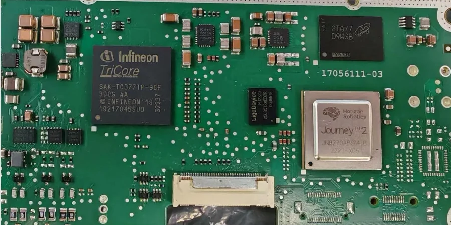
LiDAR interface board assembly is the PCB and PCBA integration of a LiDAR module's optical-transmitter support, sensitive receive electronics, timing and data processing, vehicle communication, power conversion, and diagnostics. Its engineering challenge is coexistence: low-level receive signals, fast laser-driver current edges, high-speed digital links, switching power, heat, and mechanical alignment must work together without corrupting range data or reliability evidence.
Key Takeaways
- The optical wavelength—commonly 905 nm or 1550 nm—does not directly select the PCB laminate; electrical edge rate, route length, loss/phase budget, thermal load, and manufacturability do.
- HDI, rigid-flex, low-loss laminate, heavy copper, conformal coating, and 100% X-ray are design choices, not automatic LiDAR requirements.
- AEC-Q100 and AEC-Q102 qualify semiconductor components. They do not qualify a populated LiDAR board, optical module, perception function, or vehicle.
- Build the control plan around failure mechanisms: receive-chain noise, timing jitter, power/ground coupling, hidden-joint defects, contamination, flex damage, thermal resistance, and interface margin.
- Release evidence must climb from PCB fabrication and assembly inspection to powered board test, module environmental/EMC validation, optical calibration, and system safety approval.
Table of Contents
- What does a LiDAR interface board integrate?
- How should materials and stackup be selected?
- Mixed-signal layout and power integrity priorities
- LiDAR PCBA process-control matrix
- What should LiDAR board testing prove?
- Automotive standards and responsibility boundaries
- NPI gates and requalification triggers
- Common LiDAR interface board failures
- LiDAR interface board assembly RFQ checklist
- What can HILPCB support?
- Frequently asked questions
What Does a LiDAR Interface Board Integrate?
LiDAR architectures vary—scanning, flash, time-of-flight, frequency-modulated, central-processing, or remote-sensor—but the interface board normally connects several electrically incompatible domains. Define them before discussing layer count or materials.
| Functional domain | Dominant PCB/PCBA risk | Evidence needed beyond visual inspection |
|---|---|---|
| Photodetector, TIA, ADC/TDC receive chain | Leakage, coupled switching noise, input capacitance, timing error | Noise floor, timing/calibration data, controlled leakage/cleanliness evidence |
| Laser/VCSEL driver and bias | High di/dt loop inductance, overshoot, thermal path, EMI coupling | Electrical pulse/current waveform and optical-module validation under defined load |
| FPGA/SoC, memory, clocking | PDN impedance, return discontinuity, crosstalk, BGA escape | SI/PI review, rail sequencing, programming, interface and memory test |
| Vehicle data link | Channel loss/return loss, common-mode conversion, connector/cable interaction | PHY/link diagnostics, channel or compliance test for the chosen interface |
| Input power and protection | Crank/dropout, reverse polarity, conducted transients, inrush, ground shift | Power-state and transient tests at module boundary |
| Diagnostics and safety mechanisms | Undetected faults, unsafe output, incomplete traceability | Fault injection/diagnostics and system safety evidence owned by the product team |
Vehicle connectivity may use Automotive Ethernet, a proprietary SerDes, MIPI A-PHY, CAN/CAN FD, or another OEM-defined interface. Texas Instruments' automotive Ethernet guidance also shows that data and power can share single-pair wiring through PoDL, but the coupling/decoupling network then becomes part of both the signal-integrity and power-protection design. The assembly drawing and test plan must identify the actual interface, not merely say “high speed.”
How Should Materials and Stackup Be Selected?
Start with measurable channel, power, thermal, density, and mechanical budgets. Standard or higher-performance FR-4 may be sufficient for short, well-controlled digital routes; a low-loss laminate becomes justified when modeled and measured margin cannot be met with the selected construction. Optical wavelength alone is not that justification.
| Technology choice | Use it when | Do not assume | Required evidence |
|---|---|---|---|
| FR-4 or higher-performance epoxy | Loss, phase, thermal, and reliability budgets close with available constructions | Every LiDAR receive or driver trace needs Rogers material | Material properties tied to frequency/method, solver results, fabrication coupon correlation |
| Low-loss or hybrid laminate | Insertion loss, phase stability, or edge fidelity needs it | A hybrid stackup is automatically cheaper or more reliable | Bonding compatibility, copper profile, Dk/Df basis, lamination and requalification plan |
| HDI PCB | Fine-pitch escape, compact routing, or via-stub reduction requires build-up layers | Every 0.5/0.65 mm BGA demands the same 1+N+1 or 2+N+2 build | Escape study, via reliability structure, sequential-lamination and inspection plan |
| Rigid-flex PCB | A controlled 3D interconnect can remove connectors or harnesses | Removing connectors guarantees lower cost or vibration life | Bend geometry, copper orientation, stiffener/transition design, assembly fixture and flex handling |
| Heavy copper/thermal features | Current density or spreading analysis supports them | More copper always improves thermal performance without SI or assembly trade-offs | Thermal model, current path, plane balance, solderability and warpage review |
For a low-loss or high-frequency PCB, record the laminate grade, construction, foil profile, pressed dielectric targets, solder-mask state, impedance classes, and any prohibited substitutions. “Rogers or equivalent” is too vague when the electrical model depends on a particular property definition and copper interface.
Mixed-Signal Layout and Power Integrity Priorities
The receiver front end should be protected from laser-driver, converter, clock, memory, and vehicle-interface currents. Protection comes from controlled return paths, compact current loops, thoughtful placement and layer references, adequate power filtering, and verified coupling—not from blindly splitting every ground plane. A split that forces a high-speed return current around a gap can create more radiation and jitter than it removes.
Use the actual edge spectrum and channel budget to specify impedance, loss, skew, via transitions, connectors, and reference planes. TDR coupon results support fabrication control; they do not prove a populated SerDes or Ethernet channel. Retain model-to-coupon-to-assembled-channel correlation where the interface margin is tight.
Power integrity must cover steady-state load, laser pulse demand, processor transients, startup/shutdown, brownout behavior, and external disturbances. Keep the laser-current loop and switching converter hot loops small, provide local energy storage from a calculated transient target, and verify that rail droop or ground bounce does not shift receive timing. Thermal-pad and heatsink paths must be evaluated as complete junction-to-ambient systems rather than by copper area alone.
Mechanical and optical requirements also reach the PCBA. Fiducials, connector position, board outline, fastener keep-outs, flatness, depanelization direction, optical-window contamination controls, and calibration features belong in the data package. PCB assembly cannot correct an optical tolerance stack that was never allocated.
LiDAR PCBA Process-Control Matrix
The following matrix is the article's practical release asset. Convert it into a product-specific control plan; coverage and limits must come from design risk, package guidance, customer requirements, and process validation.
| Manufacturing risk | Required design input | Process control | Release evidence / owner |
|---|---|---|---|
| Fine-pitch BGA/QFN/LGA soldering | Land pattern, stencil constraints, package warpage data, paste/alloy | SPI, placement verification, profiled reflow; nitrogen only if the validated process needs it | First-article data, inspection records, profile; assembler/customer approve |
| Hidden joints and exposed thermal pads | Package-specific void/stand-off criteria and thermal model | Defined 2D/3D X-ray or CT coverage; destructive analysis when justified | Images/data tied to serial/lot; no universal 25% void limit |
| Moisture-sensitive components | MSL, floor life, packaging and rework instructions | Receiving, dry storage, exposure tracking and bake only per applicable component rules | J-STD-020/J-STD-033 records; assembler owns control |
| Flux and ionic contamination | Flux chemistry, cleaning compatibility, leakage/use-environment risk | Qualified no-clean or wash process, handling controls, targeted cleanliness verification | Objective process evidence; ROSE alone is not universal proof |
| Optical surfaces and connectors | Cleanliness class, protected zones, cap/removal sequence | Particle/chemical controls, local inspection, packaging and handling | Optical/module inspection owned by customer or qualified integrator |
| Conformal coating or potting | Material, thickness, keep-outs, cure, rework and compatibility | Selective application, masking, cure verification, inspection | Coverage/cure data; product team validates electrical, optical and environmental effects |
| Rigid-flex installation | Bend radius, bend count, neutral-axis intent, fixture and fastener sequence | Controlled forming, no unsupported creasing, continuity/visual checks | Assembly record and mechanical validation |
| Programming and traceability | Firmware/configuration revision, key handling, serial schema, test limits | Controlled programming, checksum/readback, station and material-lot capture | Unit history and test result linked to released revision |
AOI sees accessible surface features; it cannot see every BGA or bottom-terminated joint. X-ray reveals geometry and density differences but does not by itself prove intermetallic quality, fatigue life, or thermal performance. Specify inspection purpose, coverage, decision limits, false-call handling, and retention instead of demanding “100% inspection” without defining what is inspected.
What Should LiDAR Board Testing Prove?
Testing should progress from inexpensive structural checks to product-specific evidence. A mature plan separates defect screening from design qualification and from final compliance.
| Gate | What it proves | Example evidence | What it does not prove |
|---|---|---|---|
| Bare PCB | Fabrication matches agreed construction/netlist | Electrical test, impedance coupon if specified, microsection, material/lot records | Assembly or module performance |
| Assembly workmanship | Components and soldering meet released criteria | SPI/AOI/X-ray plan, profile, first article, cleanliness/process records | Optical ranging accuracy or lifetime |
| Powered PCBA | Rails, current, programming and accessible functions operate | Shorts/current checks, boundary scan/ICT/flying probe where suitable, firmware and link loopback | Vehicle EMC, environment, eye safety |
| LiDAR module | Electronics, optics, mechanics and thermal design work together | Noise/timing, optical pulse, calibration, link margin, thermal and power-state tests | Vehicle-level perception safety |
| Environmental/EMC qualification | Module survives its mounting-location mission profile | OEM/ISO test reports, post-stress functional and parametric comparison | All vehicle integration scenarios |
| System release | Safety goals and intended perception function are adequately validated | Functional-safety and SOTIF work products, vehicle tests, release approval | Transferable approval for unrelated designs |
Environmental profiles must come from mounting location, mission profile, OEM specification, and risk analysis. Do not copy a universal -40°C to 125°C range, 85/85 exposure, cycle count, vibration spectrum, or 15-year/300,000-km claim. Define preconditioning, powered state, monitoring, sample selection, failure criteria, and post-stress measurements.
Automotive Standards and Responsibility Boundaries
AEC-Q100 covers stress-test qualification for automotive integrated circuits, while AEC-Q102 covers optoelectronic semiconductors such as photodiodes and laser components. Selecting qualified parts is useful evidence, but it does not qualify their solder joints, PCB, firmware, optical alignment, enclosure, or application.
Likewise, ISO 26262 addresses malfunctioning behavior in safety-related road-vehicle E/E systems, while ISO 21448 addresses safety of the intended functionality, including performance insufficiencies in complex sensors and processing. ISO 21448 explicitly does not cover LiDAR beam eye-damage hazards; laser-product safety is a separate system responsibility associated with IEC 60825-1.
Reference standards and specifications:
- ISO 26262 — ISO
- ISO 21448 — ISO
- ISO 16750-1, ISO 16750-3, ISO 16750-4 — ISO
- ISO 7637-2 and ISO 11452 series — ISO
- CISPR 25 — IEC/CISPR
- IEC 60825-1 — IEC
- AEC-Q100 and AEC-Q102 — Automotive Electronics Council
- IPC-6012, IPC-2221 and IPC-2223 — IPC
- J-STD-001, IPC-A-610, J-STD-020 and J-STD-033 — IPC/JEDEC as applicable
The customer or designated product authority owns safety requirements, optical safety, module/vehicle compliance, and final release. The PCB fabricator and assembler own only the agreed manufacturing controls and evidence within their contracted scope.
NPI Gates and Requalification Triggers
Names vary by organization, but an EVT/DVT/PVT-style sequence prevents production controls from being confused with design proof.
- Engineering verification: confirm architecture, bring-up, interfaces, timing/noise assumptions, thermal paths, DFM/DFA findings, and test access.
- Design validation: freeze representative hardware and verify the module against electrical, optical, mechanical, environmental, EMC, safety-derived, and diagnostic requirements.
- Production validation: prove tooling, fixtures, programming, line balance, process windows, measurement capability, traceability, packaging, and reaction plans on the intended production flow.
Define requalification triggers in the control plan. Review material or supplier changes, PCB stackup and copper changes, component PCNs, package/land-pattern changes, stencil or paste changes, reflow and cleaning changes, coating/potting changes, fixture/software revisions, manufacturing-site transfers, and adverse yield or field trends. Risk determines which evidence must repeat.
Common LiDAR Interface Board Failures
| Symptom | Likely contributors | Useful isolation evidence |
|---|---|---|
| Range jitter or elevated receive noise | Driver/clock coupling, rail droop, leakage, grounding or timing error | Correlated rail, current-pulse, receive-noise and timing captures |
| Ethernet/SerDes link is marginal after assembly | Connector/launch, pair asymmetry, PoDL network, common-mode conversion, solder defect | PHY diagnostics, channel data, TDR/time-domain localization, X-ray as relevant |
| Intermittent BGA failure after stress | Warpage, head-in-pillow, pad/crack, rework or CTE strain | X-ray/CT, cross-section or dye analysis under an approved failure-analysis plan |
| Humidity leakage or corrosion | Residue, moisture path, coating defect, exposed bias nodes | Ionic/chemical analysis, insulation monitoring and process history |
| Rigid-flex open after installation | Bend violation, transition stress, copper orientation, fastener load | Continuity during forming, section review and mechanical recreation |
| Thermal shutdown or calibration drift | Incomplete pad soldering, interface resistance, airflow/enclosure assumption | Thermal map, power data, X-ray, junction/board/ambient correlation |
| Reset during vehicle disturbance | Protection/hold-up weakness, ground shift, firmware recovery | Input/rail/reset waveforms during specified transient test |
LiDAR Interface Board Assembly RFQ Checklist
Design package
- ODB++/IPC-2581 or Gerber and drill data, netlist, stackup, fabrication drawing, BOM/AVL, centroid data, assembly drawings, schematics, 3D/mechanical model, panel requirements, and revision identifiers.
- Impedance/loss requirements, controlled interfaces, via/backdrill structures, material and substitution rules, thermal/ground strategy, coating and optical keep-outs.
Assembly and test
- Package MSL and handling rules, stencil/paste/alloy requirements, reflow constraints, inspection coverage and acceptance source, cleanliness objective, coating/potting process, depanelization and flex-forming instructions.
- Programming package, test software/fixtures, rail/current limits, interface loopback, calibration handoff, fault logging, golden units, sample plan, data format and retention.
Quality and production
- Applicable IPC class and customer addenda, approved process/supplier list, traceability depth, first-article/PPAP expectations, nonconformance authority, change-notification period, requalification triggers, EAU/lot definition, packaging, shelf-life and delivery plan.
What Can HILPCB Support?
HILPCB can review the PCB and assembly data package, coordinate stackup and coupon requirements, identify manufacturability and assembly risks, and align the agreed process-control, inspection, traceability, and test-data package for turnkey assembly. Exact equipment, inspection coverage, automotive quality-system requirements, functional fixtures, environmental tests, optical calibration, and external-laboratory deliverables must be confirmed during quotation.
HILPCB does not replace the customer's LiDAR design authority, semiconductor qualification review, functional-safety process, SOTIF validation, laser-safety assessment, vehicle EMC/environmental approval, or final product release. Send the complete RFQ checklist—not only Gerbers and a BOM—to receive a quote based on the real control plan.
Frequently Asked Questions
Does every LiDAR interface board require a low-loss laminate?
No. Select material from electrical edge rate, route length, insertion-loss/phase budget, temperature behavior, copper profile, cost, and fabrication correlation. Optical wavelength alone does not make Rogers or another RF laminate mandatory.
When is HDI justified for a LiDAR board?
HDI is justified when package escape, routing density, via-stub, or module-size constraints cannot be met reliably with conventional through vias. The BGA pitch alone does not determine the required build-up sequence.
Is rigid-flex always more reliable than connectors?
No. Rigid-flex can reduce connector count and assembly steps, but it introduces bend, transition, lamination, handling, and repair constraints. Compare validated mission-profile reliability and total installed cost for both architectures.
Does AEC-Q100 make a LiDAR PCBA automotive-qualified?
No. AEC-Q100 qualifies integrated circuits to its scope. The populated board and LiDAR module still require assembly-process evidence plus product-specific electrical, environmental, EMC, optical, and safety validation.
Which LiDAR PCBA inspections should be 100%?
There is no universal list. Define coverage from failure risk and detection capability. SPI, AOI, X-ray, electrical test, programming, and functional test detect different defects; “100%” must name the unit, feature, method, and acceptance rule.
Build a Traceable Release Case
Reliable LiDAR interface board assembly comes from linked evidence: requirements drive architecture, design risks drive process controls, process controls produce traceable data, and module/system tests close the safety and performance argument. Provide HILPCB with the released files, NPI gate plan, inspection criteria, test ownership, and change-control rules for a manufacturing review and quotation grounded in your actual LiDAR product.