
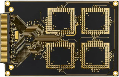
An eight-inch channel does not become qualified when its drawing says Megtron 6 or Megtron 7. The choice depends on the loss budget, the core and prepreg around each signal layer, copper roughness, vias and connectors. Choose the lowest-cost approved construction that meets the complete channel requirements with margin; a lower datasheet dissipation factor alone cannot establish that margin.
Panasonic's MEGTRON family includes multiple glass and processing variants within each grade. The material callout must identify those variants before an impedance model or supplier quote becomes useful. For comparisons across material families, start with low-loss PCB selection. The decision here is narrower: which Panasonic construction to model, purchase and verify before an engineering validation build (EVT).
Which Megtron 6 or Megtron 7 part number belongs on the drawing?
Panasonic Megtron 6 uses R-5775 laminate and R-5670 prepreg designations, with suffixes identifying different constructions. MEGTRON6 is the manufacturer's compact family spelling; an order saying only that name leaves the glass type and construction unresolved.
| Family and glass | Laminate / prepreg pair | What the suffix tells the buyer |
|---|---|---|
| Megtron 6, normal glass | R-5775(K) / R-5670(K); R-5775(G) / R-5670(G) | K and G have their own construction tables; select the actual core and prepreg rather than assuming interchangeability |
| Megtron 6, low-Dk glass | R-5775(N) / R-5670(N) | N identifies the low-Dk glass version |
| Megtron 7, low-Dk glass | R-5785(N) / R-5680(N); new R-578Y(N) / R-568Y(N) | Existing and new part numbers appear together on the current product page |
| Megtron 7, low-Dk glass with improved processability | R-5785(GN) / R-5680(GN); new R-578Y(GN) / R-568Y(GN) | GN has a separate construction and foil reference from N |
| Megtron 7, normal glass with improved processability | R-5785(GE) / R-5680(GE); new R-578Y(GE) / R-568Y(GE) | GE is not the low-Dk glass version |
Sources: Panasonic's current MEGTRON6 and MEGTRON7 product pages. Panasonic also lists buried-resistor copper-foil laminates: R-5775(S), low-Dk glass; R-5775(R), normal glass; and R-5785(R)/R-578Y(R) in MEGTRON7. These suffixes do not describe ordinary copper roughness classes, and the pages do not list matching S/R prepreg pairs.
For MEGTRON7, Panasonic warns that UL certification conditions may differ between existing and new part numbers. Confirm the supplied label, applicable recognition conditions and drawing approval before accepting a new designation. A similar name or typical Dk is insufficient substitution evidence.
What does the Megtron 6 datasheet say at 10 GHz?
For Panasonic Megtron 6, dielectric constant (Dk) describes the dielectric response used in propagation and impedance models. Dissipation factor (Df), also called loss tangent, describes dielectric loss. Neither parameter includes all conductor, via or connector losses.
The manufacturer-hosted April 2021 R-5775/R-5670 datasheet, No. 21041931, gives the following R-5775 general-property values. Its reference sample is 0.750 mm thick, Core Type 30; the electrical conditioning code is C-24/23/50. Values are typical, not guaranteed.
Panasonic Megtron 6 Dk Df 10 GHz general-property rows from the R-5775/R-5670 datasheet:
| Frequency | Dk | Df / loss tangent | Published test method |
|---|---|---|---|
| 1 GHz | 3.71 | 0.002 | IPC-TM-650 2.5.5.9 |
| 10 GHz | 3.61 | 0.004 | IPC-TM-650 2.5.5.5 |
Source: Panasonic R-5775/R-5670 datasheet, physical page 2. Do not take the 1 GHz value of 0.002 and label it a 10 GHz loss tangent. Conversely, this two-row table is not a controlled measurement of frequency dependence alone: the test method also changes.
These are the Panasonic Megtron 6 dielectric constant and dissipation factor values most procurement requests actually need: Dk 3.61 and Df (loss tangent) 0.004 at 10 GHz. When a request asks only for the Panasonic Megtron 6 loss tangent 10 GHz figure, return it with its test method and sample condition attached — the 1 GHz row uses a different method and is not interchangeable.
Why the core construction changes Dk
The same datasheet's R-5775(K) core table provides these 10 GHz values using IPC-TM-650 2.5.5.5. Each row has its own thickness; the 0.750 mm general-property sample condition does not apply to every row.
| Glass style | Plies | Typical resin content | Core thickness | Dk at 10 GHz | Df at 10 GHz |
|---|---|---|---|---|---|
| 1035 | 1 | 65% | 0.050 mm | 3.37 | 0.004 |
| 1078 | 1 | 63% | 0.075 mm | 3.39 | 0.004 |
| 3313 | 1 | 54% | 0.100 mm | 3.61 | 0.004 |
| 1035 | 2 | 65% | 0.100 mm | 3.37 | 0.004 |
| 2116 | 1 | 54% | 0.125 mm | 3.61 | 0.004 |
| 2116 | 6 | 54% | 0.750 mm | 3.61 | 0.004 |
Source: the same Panasonic datasheet, physical page 3. The two 0.100 mm cores differ in Dk by 0.24: 3.61 minus 3.37. Equal dielectric thickness and the same family name therefore do not identify an equivalent impedance construction.
Prepreg needs its own data. For example, the R-5670(K) prepreg table lists 1035 glass at 70% resin and 60 µm typical thickness with Dk 3.23 and Df 0.004 at 10 GHz. That is a different construction from the 1035 core rows above. Ask for the proposed pressed thickness, resin content and model values around the signal layer. The impedance calculator can help estimate starting geometry; final dimensions need the fabricator's approved stackup and the agreed verification method.
How do the current 13–14 GHz properties compare?
Panasonic's current product pages use a balanced-type circular disk resonator, C-24/23/50 conditioning and a 0.75 mm sample. Keep the frequency attached to each value when comparing grades.
| Material on current product page | Glass | Frequency | Typical Dk | Typical Df |
|---|---|---|---|---|
| R-5775(K) / R-5775(G) | Normal | 13 GHz | 3.62 | 0.0046 |
| R-5775(N) | Low-Dk | 13 GHz | 3.34 | 0.0037 |
| R-5785(GE) / R-578Y(GE) | Normal | 13 GHz | 3.60 | 0.0034 |
| R-5785(N), R-5785(GN) and corresponding R-578Y versions | Low-Dk | 14 GHz | 3.31 | 0.0023 |
The MEGTRON7(G) April 2022 datasheet, No. 22040128, also gives GE 3.60/0.0034 at 13 GHz and GN 3.31/0.0023 at 14 GHz. Its method note identifies IEC 63185 (2020). Those figures are not 10 GHz values. A historical sheet with another frequency is not automatically wrong; preserve its document identity and conditions rather than combining it with this table.
The current MEGTRON7 page identifies H-VLP copper for the N reference and H-VLP2 for GN/GE. The MEGTRON6 general-property reference uses H-VLP. Treat these as specified test configurations, not a complete availability list or a guarantee for any foil sold under the family name. Request the actual foil designation and roughness model used in channel simulation. Copper foil treatment and the board's final surface finish are separate choices.
Thermal data also need their methods: current pages list Tg by DSC at 185°C for MEGTRON6 and 200°C for MEGTRON7, and T288 with copper greater than 120 minutes under IPC-TM-650 2.4.24.1, condition A. These are typical material-test results, not maximum operating temperatures or guarantees for a specified number of reflow cycles. The finished stackup, plated holes and assembly profile still need their own qualification.
Can an eight-inch channel meet the loss budget?
Start with the actual serial line rate per lane. NRZ carries one bit per symbol; PAM4 carries two. For a line rate R in Gb/s, the corresponding Nyquist frequency is R/2 GHz for NRZ and R/4 GHz for PAM4. Thus 28 Gb/s NRZ and 56 Gb/s PAM4 both have a 14 GHz Nyquist frequency; 112 Gb/s PAM4 has 28 GHz. Use the encoded line rate, including the applicable coding or FEC overhead, rather than application payload throughput. Nyquist is a reference frequency, not the entire measurement bandwidth. Keysight's signal-parameter definitions explain the bit/symbol distinction.
Consider an illustrative allocation at 14 GHz, using positive loss magnitudes. Assume an 8-inch board route, a 6 dB total insertion-loss allowance at the chosen reference planes, 2 dB allocated to other path elements, and 1 dB reserved margin. The route allocation is:
(6 dB − 2 dB − 1 dB) / 8 in = 0.375 dB/in
If a model correlated to the proposed construction gives 0.30 dB/in, the allocation totals 8 × 0.30 + 2 + 1 = 5.4 dB. At 0.45 dB/in, it totals 6.6 dB, exceeding the assumed allowance. These slopes are hypothetical inputs, not measured Megtron 6 or Megtron 7 specifications. They show what the supplier's construction data must resolve before a price comparison can settle the material choice.
This scalar calculation screens the loss allocation. A real channel requires cascaded models with consistent reference planes and checks for reflections, crosstalk, mode conversion, transmitter/receiver behavior and the applicable eye or error-rate requirement. Discontinuities can produce resonances that a sum of nominal dB values misses. The signal attenuation discussion covers the separate loss mechanisms.
Which failure needs a material change, and which needs a different test?
| Observation | First investigation | Evidence that supports the next decision |
|---|---|---|
| Impedance is acceptable but insertion loss is excessive | Confirm foil/model, dielectric construction, trace geometry, launches and de-embedding | Frequency-domain insertion loss for a representative structure, correlated with the model; impedance alone is insufficient |
| A narrow loss notch appears near a via transition | Inspect residual barrel, pads, antipads and return-path geometry | Via model and measured response over the required band; residual-stub measurement where backdrilling is specified |
| Differential timing or mode conversion varies with routing orientation | Check glass construction, weave exposure, geometry and pair symmetry | Skew and mixed-mode measurements or simulation against the project's timing/channel allocation |
| Blistering, pad separation or plated-hole damage follows thermal exposure | Identify the failure interface, moisture/handling history, actual process and thermal profile | Targeted cross-section and agreed thermal/reliability evidence, using the applicable drawing and acceptance requirements |
| Hybrid stackup differs from the approved build | Review both dielectric sides of each signal, cure compatibility, resin fill and expansion | Revised stackup, process review, channel model and agreed requalification before substitution |
A via stub cannot be assigned a universal resonance from its length alone. For an ideal uniform open stub, f ≈ c / (4L√εeff). With the explicitly assumed εeff = 3.6 and c ≈ 3.00 × 10⁸ m/s, a 0.5 mm stub gives about 79 GHz; 13 GHz corresponds to about 3.04 mm. Real via pad loading and field geometry change that estimate, and a stub can degrade a channel below its first resonance. This is a sanity check, not a permissible residual-stub specification. TI's High-Speed Layout Guidelines, SCAA082A, section 2.5 describes the open-stub resonance mechanism.
An ordinary coupon TDR impedance report checks the agreed impedance measurement. It does not independently establish Df or full-channel insertion loss. Dk extraction, propagation measurement and loss characterization require defined test structures, calibration and methods; suitable TDR/TDT or network-analyzer techniques can supply more than impedance when configured for that purpose. State the requested result and method in the purchase package instead of asking vaguely for a “coupon test.” For thermal separation, use the failure analysis route in PCB delamination.
What should the quote and release package contain?
Lock the material approval record to the board revision. Include laminate and prepreg part numbers with suffixes, glass styles and resin content, layer-by-layer pressed thicknesses, foil type and thickness, impedance geometries, allowable substitutions and the applicable material specification. The IPC-4101 material specification discussion explains why a specification callout and a trade name serve different purposes.
Ask the supplier to separate material procurement, fabrication, first-article evidence and recurring inspection costs. A quote should identify the offered construction, available quantity, procurement timing and quote validity. Core/prepreg combinations, panel utilization, backdrilling or sequential lamination, and the chosen test scope can change cost independently of the Megtron grade. A hybrid build may reduce material spending, but its process compatibility and electrical behavior require approval for the whole stackup. Do not approve a substitution solely because its headline Df is lower.
Before EVT fabrication, the designer approves the stackup and channel assumptions; the fabricator confirms the proposed process and material availability; quality agrees the test structures, methods, sampling and acceptance criteria. The first build then supplies the evidence defined in that plan. System validation remains the product team's responsibility. Any change to construction, foil or supplier after that point needs an assessed revalidation scope; EVT, DVT and production labels do not impose a universal inspection schedule.
For a high-speed PCB or multilayer PCB quotation, send the fabrication files, proposed stackup, actual line rate and modulation, critical route lengths, impedance targets and channel allocation. Include the reports needed for release and any restriction on material substitutions. Submit the package through the quote request; material availability, process feasibility and evidence deliverables should be confirmed for that project before the order is released.
FAQ
What is Megtron 6?
Megtron 6 is Panasonic's low-loss multilayer PCB material family. Its R-5775 laminates and R-5670 prepregs include normal-glass K/G and low-Dk-glass N variants. Specify the variant and construction because the family name alone does not define Dk, foil or finished-board performance.
What are Panasonic Megtron 6 Dk and Df at 10 GHz?
Panasonic's April 2021 R-5775/R-5670 datasheet gives typical Dk 3.61 and Df 0.004 at 10 GHz for the 0.750 mm general-property sample, using IPC-TM-650 2.5.5.5 and C-24/23/50 conditioning. Its construction tables contain other Dk values, so match the actual core or prepreg before using the number in a model.
Is the Megtron 6 loss tangent 0.002 or 0.004?
Both appear in the cited R-5775 general-property table: 0.002 at 1 GHz under IPC-TM-650 2.5.5.9 and 0.004 at 10 GHz under 2.5.5.5. Loss tangent is another name for Df. Keep the method and frequency with the value; neither number describes every MEGTRON6 construction at every frequency.
When should I choose Megtron 7 instead of Megtron 6?
Choose an approved Megtron 7 construction when its modeled and verified channel performance provides the margin the design needs at an acceptable project cost. There is no universal length or data-rate boundary. Compare the exact dielectric and foil constructions, including process and substitution approval, rather than only the family names.
Does a passing TDR coupon prove the channel will work?
A passing impedance coupon establishes the result defined by that measurement plan. It does not by itself prove dielectric loss, insertion loss or receiver performance. Request the appropriate propagation or S-parameter evidence and validate the complete channel against the system requirements.
Can a supplier substitute a new Megtron 7 part number?
Only after the change is reviewed and approved for the build. Panasonic lists R-578Y/R-568Y alongside existing R-5785/R-5680 numbers and warns that UL certification conditions can differ. Match the exact suffix, construction, foil and applicable recognition conditions, then assess any required electrical or reliability revalidation.