
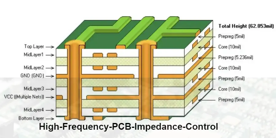
Introduction: Why IPC-4101 is the foundation of PCB design
IPC-4101, Specification for Base Materials for Rigid and Multilayer Printed Boards, is the industry’s “gold standard” for defining PCB core materials—copper clad laminates (CCL) and prepregs (PP): performance, minimum requirements, and test methods. It classifies different material performance levels via “Slash Sheets”—from general-purpose FR-4 to high-speed low-loss laminates—giving designers and manufacturers a shared language.
But knowing the Slash Sheet number is only the start. In real stackup design, impedance simulation, and production, questions around IPC-4101 never stop: why do measured Dk/Df differ from the datasheet? why does a hybrid stackup delaminate? how do you balance cost vs. performance? This stackup faq answers 20 core questions related to ipc 4101 specification guide, helping you handle the full workflow—from material selection to volume delivery.
Stackup & material FAQ quick index
| No. | Topic | Key metrics | Core recommendation |
|---|---|---|---|
| 1-5 | Basic material selection | Tg, Td, Dk/Df, CTE | Choose the right Slash Sheet based on temperature, data rate, and budget. |
| 6-9 | High-speed / RF design | Dk vs. frequency, glass weave effect, copper roughness | Prefer spread glass and low-profile copper; use 3D field simulation when needed. |
| 10-14 | Lamination & manufacturing | resin content, press parameters, copper balance | Confirm resin flow model with the fab; keep copper distribution symmetric. |
| 15-18 | Impedance & reliability | TDR, TCDk, CAF | Include solder mask and temperature drift; validate with impedance coupon. |
| 19-21 | Special materials | PI Dk, thermal conductivity, CTE matching | FPC: dynamic bend; MCPCB: thermal path; hybrid: CTE compatibility. |
Part 1: Basic material selection & parameter decoding (FAQ 1-5)
Q1: What is an IPC-4101 “Slash Sheet”, and how do you use it?
- Question: I often see IPC-4101/126, /21, etc. What do they mean?
- Typical scenario: Choosing among dozens of vendor materials and not knowing which one matches the design requirement.
- Key metrics/tests: Tg (glass transition), Td (decomposition), Dk (dielectric constant), Df (loss tangent), CTE (coefficient of thermal expansion).
- Solution: Each Slash Sheet number corresponds to a set of minimum performance requirements. For example:
- /21: Standard Tg (≥110°C) epoxy FR-4 for consumer electronics.
- /126: High Tg (≥170°C) epoxy FR-4 for lead-free reflow, automotive, and servers.
- /99: Halogen-free high Tg FR-4 for environmental compliance. Designers should select the Slash Sheet based on thermal stress (e.g., reflow peak), operating environment, and SI requirements. Then, among materials compliant with that Slash Sheet, pick a specific model based on cost and availability (e.g., ITEQ IT-180A is within /126).
- Prevention: Early in the project, specify the required IPC-4101 Slash Sheet in the schematic/design spec, rather than locking a single vendor part number—this increases supply-chain flexibility.
Q2: High Tg (e.g., /126) vs. standard Tg (e.g., /21) FR-4—what’s the real difference?
- Question: If my product must pass lead-free reflow, do I have to use high Tg material?
- Typical scenario: A 4-layer board uses standard Tg FR-4 to save cost, but delamination/popcorning appears after multiple reflow cycles.
- Key metrics/tests: Tg (Glass Transition Temperature), Td (Decomposition Temperature), Z-axis CTE.
- Solution: The core difference is thermal robustness.
- Tg: the temperature where the material transitions from glassy to rubbery. High Tg materials (typically >170°C) deform less and stay more stable at elevated temperature.
- Td: temperature where the material loses 5% mass; an indicator of long-term thermal stability.
- Z-axis CTE: high Tg materials usually have lower Z-axis expansion, reducing via stress during soldering and improving PTH reliability. For lead-free processes (245–260°C peak), Tg ≥ 170°C (/126 or higher) is strongly recommended for robust soldering reliability.
- Prevention: Evaluate reflow cycles, operating temperature, and reliability targets. For high-reliability multilayer PCB, treat high Tg as the default option.
Q3: Can I trust datasheet Dk/Df values? Why does simulated impedance not match measurements?
- Question: I used the laminate vendor’s Dk=4.2 to design 50Ω, but measurement is 47Ω.
- Typical scenario: In high-speed digital, impedance mismatch causes reflections and eye diagram failures—classic
dk drift. - Key metrics/tests: Dk/Df vs. frequency, resin content, pressed thickness.
- Solution: Datasheet Dk/Df are reference values measured at specific frequency (e.g., 1GHz) and method. Real Dk depends on multiple factors:
- Frequency dependence: Dk typically decreases as frequency rises. FR-4 Dk at 10GHz can be 5–10% lower than at 1GHz.
- Resin content: PP Dk is lower than CCL core because glass fiber Dk (
6.0) is higher than resin (3.2). Effective Dk is a mixture. - Pressing effects: During lamination, PP resin flows and fills copper topography; final thickness and resin ratio shift, changing effective Dk.
Best practice: Request press-verified stackup data from a manufacturer like HILPCB, or use our HILPCB Stackup Simulation tool calibrated by massive
impedance coupondatasets.
- Prevention: Don’t use a single datasheet Dk. Ask for a stackup proposal including resin content, post-press thickness, and banded Dk values.
Q4: What are the pros/cons of Halogen Free materials?
- Question: The customer asks for RoHS + halogen-free—what should I choose?
- Typical scenario: Exporting consumer electronics into the EU and needing compliance; selecting
halogen free pcb materials. - Key metrics/tests: halogen content (Cl, Br < 900ppm each; total < 1500ppm), moisture absorption, Dk/Df.
- Solution:
- Pros: more eco-friendly; fewer toxic gases during burning; often higher Tg/Td and better thermal stability.
- Cons:
- Higher cost: typically 10–20% more than comparable halogenated systems.
- Dk/Df: Dk/Df can be slightly higher, impacting high-speed signals.
- Processability: tends to be harder/brittle, requiring tighter drilling/process control.
- Moisture absorption: some halogen-free systems absorb more moisture, affecting electrical performance and reliability. Common Slash Sheets: IPC-4101/99, /101, /129, /130 are widely used halogen-free specs.
- Prevention: Confirm compliance targets early. If halogen-free is required, work with the fab to pick a mature, stable-supply material family. If the product also needs a UL 94V-0 flammability rating, confirm the chosen laminate carries it.
Q5: What is “resin flow”, and how does it affect my design?
- Question: Why do I see pad sinking or voids under BGA after lamination?
- Typical scenario: In large copper-open areas, excessive PP resin fill causes non-uniform thickness and can even impact inner-layer features—classic
resin flowcontrol issue. - Key metrics/tests: resin content (RC%), resin flow, lamination parameters (pressure, ramp rate).
- Solution: During pressing, PP resin melts and flows from high-pressure to low-pressure regions (e.g., no-copper areas).
- High flow PP (HRC): good for fine-line fill and smoothing inner-layer topography, but may over-flow in low-copper-density zones.
- Medium flow (MRC): general-purpose.
- Low flow (LRC): for rigid-flex or embedded capacitance/resistance processes where flow must be constrained. Countermeasure: Add non-functional copper mesh in regions with large copper-density differences to balance copper and guide uniform resin flow. Also inform the fab which regions have tight thickness tolerance needs.
- Prevention: Do
high current copper balancingnot only to prevent warpage, but also to stabilize resin flow. Mark critical thickness-tolerance zones in the fabrication notes.
Stackup design getting painful?
Whether it’s a high-speed multilayer build or a complex hybrid stackup, HILPCB engineers can provide free stackup optimization suggestions and professional DFM analysis. Our HILPCB Materials Library covers hundreds of materials—from FR-4 to Rogers—so your design can meet both performance and cost targets.
Get a free stackup reviewPart 2: High-speed/RF design & signal integrity (FAQ 6-9)
Q6: When should you upgrade from FR-4 to low-loss materials like Rogers?
- Question: My data rate is above 10Gbps—can I still use FR-4?
- Typical scenario: Designing a PCIe 4.0 interface card; even with high-end FR-4 (e.g., EM-827), insertion loss is too high and the eye won’t open—typical
low loss laminate tutorial. - Key metrics/tests: insertion loss (S21), Df at target frequency.
- Solution: Upgrade decisions are driven by the loss budget (dielectric + conductor loss).
- Dielectric loss scales with Df and frequency.
- Standard FR-4 (Df ≈ 0.02): < 3Gbps.
- Mid-loss FR-4 (Df ≈ 0.01): 3–6Gbps.
- Low-loss FR-4 (Df ≈ 0.005): 6–15Gbps.
- Ultra-low loss (e.g., Rogers RO4350B, Df ≈ 0.0037): > 15Gbps and mmWave. Decision point: If the channel is long and simulation shows FR-4 can’t meet the loss budget, upgrade to Rogers (or equivalent).
- Dielectric loss scales with Df and frequency.
- Prevention: Run early channel simulation. If loss margin is < 3dB, consider material upgrade or routing optimization.
Q7: What is the glass weave effect, and how do you mitigate it?
- Question: Why do two differential pairs show very different delay skew?
- Typical scenario: In 28Gbps SerDes, skew increases ISI and BER.
- Key metrics/tests: effective Dk variation, intra-pair skew.
- Solution: PCB dielectric is a mix of glass fiber (Dk≈6.0) and resin (Dk≈3.2). If one trace rides on glass bundles while the other rides on resin windows, effective Dk differs and delay diverges.
- Mitigation 1 (routing): route differential pairs at 10–15° (zig-zag) so both traces sample similar glass/resin environments.
- Mitigation 2 (material): choose flatter, tighter glass styles (e.g., 1067/1086 better than 7628), or mechanically spread glass.
- Mitigation 3 (rotation): rotate the full design slightly (e.g., 5–10°) at panel level.
- Prevention: For >10Gbps, prefer spread-glass materials and include zig-zag/small-angle rules in routing constraints.
Q8: How does copper roughness (copper profile) impact high-speed loss?
- Question: I used a good low-loss dielectric—why is HF loss still worse than expected?
- Typical scenario: A 5G mmWave antenna board; simulated vs. VNA S21 deviates significantly above 20GHz.
- Key metrics/tests: copper roughness (Rz, Rq), skin effect.
- Solution: At high frequency, current concentrates near conductor surface (skin effect). Rough copper increases path length and adds conductor loss.
- Standard RTF: rougher; strong peel strength; good for general products.
- VLP: lower roughness; common for high-speed digital.
- HVLP: ultra-low roughness; for 56/112G PAM4 and mmWave. Selecting VLP/HVLP can significantly reduce insertion loss at high frequency. Tradeoff: smoother copper has lower peel strength and requires tighter lamination control.
- Prevention: Specify copper type/roughness (inner + outer), not only dielectric material.
Q9: What is a hybrid stackup, and what are the risks?
- Question: To save cost, can I mix FR-4 and Rogers in one stackup?
- Typical scenario: An 8-layer board with RF front-end + digital; use Rogers only on RF-related outer layers, FR-4 in the core.
- Key metrics/tests: CTE compatibility, press-window compatibility, delamination test (TMA).
- Solution: Hybrid stackups are feasible and commonly used to balance cost vs. performance, but risks matter:
- CTE mismatch: different CTEs create internal stress during thermal cycling, causing delamination or via cracks.
- Complex lamination: different materials want different temperature/pressure/time; the fab must have hybrid experience.
- Chemical compatibility: processes like De-smear can affect materials differently and weaken hole-wall bonding. HILPCB recommendation: pick compatible CTE combinations (e.g., RO4350B + high Tg FR-4). Our HILPCB Hybrid Lamination Lab has mature parameters for hundreds of hybrid combinations, improving yield and reliability.
- Prevention: Confirm hybrid feasibility early and obtain recommended material combos and stackup structure.
Risk note: the hidden cost of hybrid stackups
Hybrid stackups can lower material cost, but process complexity and reliability risks may increase manufacturing cost and lead time. Immature hybrid lamination can cause yield swings in volume builds and even early field failures. Before choosing a hybrid approach, evaluate total lifecycle cost—not only laminate purchasing cost.
Part 3: Manufacturing process & DFM considerations (FAQ 10-14)
Q10: Why is my final board thickness out of tolerance?
- Question: I designed 1.6mm but received 1.75mm.
- Typical scenario: Mechanical enclosure is tight; thickness out-of-spec prevents assembly.
- Key metrics/tests: post-press dielectric thickness, copper thickness, solder mask thickness.
- Solution: Total thickness is the sum of core, PP, copper, and coatings (mask/legend). Common causes:
- PP press-out thickness estimation error: final PP thickness depends on glass style, resin content, and copper pattern density on both sides; fabs compensate using experience and simulation tools.
- Copper thickness: inner copper is more standard; outer plating adds copper, especially around holes.
- Solder mask thickness: non-uniform; thinner near pads and thicker over no-copper areas (often 0.5–1.5mil). Countermeasure: confirm expected “post-lamination” thickness per dielectric with the fab. If you need tight thickness tolerance (e.g., ±5%), call it out at order.
- Prevention: Provide a complete stackup drawing (materials, thicknesses, copper weights, impedance requirements) and co-review with the CAM engineer.
Q11: How do you design effective copper balancing?
- Question: My multilayer boards always warp upward after fabrication.
- Typical scenario: A 12-layer server board with dense power planes on one side and signal layers on the other; severe warpage blocks SMT—typical
high current copper balancingissue. - Key metrics/tests: stackup symmetry, copper coverage by layer.
- Solution: Warpage is mainly caused by asymmetric structure and uneven stress during thermal expansion/contraction.
- Structural symmetry: mirror around the center; keep dielectric thickness and copper weights similar between L1/L12, L2/L11, etc.
- Copper distribution symmetry: also keep copper density balanced within each layer. Add grounded copper mesh in sparse regions to match the opposite power plane coverage.
- Prevention: After layout, use CAM tools to analyze copper coverage per layer and adjust intentionally for symmetry.
Q12: Can I use different PP styles in one stackup?
- Question: To hit thickness/impedance, an engineer suggests 1×1080 PP + 2×2116 PP.
- Typical scenario: For a
four layer impedance controlbuild, one PP style can’t meet both thickness and impedance. - Key metrics/tests: resin flow compatibility, post-press dielectric uniformity.
- Solution: Yes—this is common. Fabs often mix PP types to fine-tune thickness and effective Dk. Example: use high-resin 1080 for fill, then 2116 to build the main dielectric thickness.
- Prevention: Let experienced PCB manufacturers own this fine stackup design. Designers provide final thickness/impedance targets; HILPCB engineers use internal databases and simulation tools to select the best PP combination.
Q13: How much does solder mask affect impedance?
- Question: My microstrip simulation is accurate—why does measured impedance drop after solder mask?
- Typical scenario: RF matching network requiring tight impedance; solder mask impact was ignored—key point in
solder mask selection tutorial. - Key metrics/tests: solder mask Dk (typically 3.0–3.8), mask thickness.
- Solution: Solder mask is dielectric. Over microstrip, it increases effective Dk and lowers characteristic impedance (often by 2–4Ω).
- Approach 1 (simulation): include solder mask layer (Dk + thickness) in impedance simulation.
- Approach 2 (design): design slightly higher (e.g., 52Ω) to compensate for the drop.
- Prevention: Use professional stackup/impedance tools (e.g., Polar Si9000) and ensure the model includes solder mask; confirm mask type/electrical params with the fab.
Q14: What is CAF, and how can material choice reduce the risk?
- Question: My high-density product leaks/shorts in high-temp/high-humidity.
- Typical scenario: 0.4mm-pitch BGA region; after long operation, adjacent vias short and crash the system.
- Key metrics/tests: CAF resistance grade, glass window size, resin system.
- Solution: CAF is a conductive filament growing inside the laminate along glass bundles from anode (+) to cathode (-). Heat, humidity, and high electric field accelerate it.
- Material choices:
- High Tg materials often have better CAF resistance.
- Small-window glass styles (e.g., 106/1080) help block CAF paths.
- Improved resin systems in modern materials are optimized for CAF resistance.
- Design rule: keep sufficient Drill-to-Copper spacing.
- Material choices:
- Prevention: For high-density, high-reliability HDI PCB, select materials explicitly rated for high CAF resistance and enforce strict spacing rules.
Part 4: Special applications & reliability validation (FAQ 15-21)
Q15: What is an impedance coupon, and do I need it?
- Question: The fab added a test strip on the panel edge—what is it?
- Typical scenario: First impedance-controlled build; unsure whether final impedance meets spec.
- Key metrics/tests: TDR (time-domain reflectometry).
- Solution: An impedance coupon (test coupon) is fabricated on the panel edge using the exact same process as the product. It includes test traces with the same parameters (width/spacing/reference) as your controlled-impedance lines. After fabrication, TDR testing on the coupon accurately represents in-board impedance—standard
impedance couponvalidation. - Conclusion: For any impedance-controlled PCB, an impedance coupon is required; it is the final evidence that manufacturing meets design intent.
Q16: How does temperature affect impedance (TCDk)?
- Question: The product works at room temp, but fails during high-temp aging.
- Typical scenario: Outdoor comms equipment degrades in summer; SI worsens.
- Key metrics/tests: TCDk (temperature coefficient of Dk).
- Solution: Most materials’ Dk increases with temperature, lowering impedance. TCDk quantifies this (ppm/°C).
- Standard FR-4: higher TCDk; more temperature sensitive.
- High-speed/RF materials: often optimized for very low TCDk for stability across wide temperature (e.g., some Rogers materials).
- Prevention: For wide-temp and impedance-stability-critical products (automotive, aerospace, outdoor), select low-TCDk materials and design for worst-case impedance drift.
Q17: What’s special about FPC material selection?
- Question: My FPC cracks after repeated bending.
- Typical scenario: A consumer product requiring dynamic flex; traces near the connector fail in life testing.
- Key metrics/tests: dynamic bend cycles, coverlay type, adhesive selection.
- Solution: FPC core dielectric is Polyimide (PI).
- Base material: adhesive vs. adhesiveless. Adhesiveless PI is thinner, more flexible, and more heat resistant—preferred for dynamic flex.
- Copper foil: use RA copper (Rolled-Annealed) for repeated bending, not ED copper.
- Coverlay: prefer adhesiveless coverlay.
- Design: use arc transitions in bend area; route traces perpendicular to the bend axis.
- Prevention: Define whether the flex is static or dynamic and choose the correct stack (adhesiveless PI + RA copper).
Q18: What are the key parameters for MCPCB?
- Question: My high-power LED board runs hot and suffers severe lumen depreciation.
- Typical scenario: A 100W LED module; even with a large heatsink, junction temperature is too high.
- Key metrics/tests: thermal conductivity (W/m·K), hi-pot (dielectric withstand).
- Solution: MCPCB centers on a thin, high-thermal-conductivity insulating layer separating circuits from the metal base (usually aluminum).
- Thermal conductivity: the most critical parameter. Standard MCPCB is ~1–3 W/m·K; high-performance can reach 5–10 W/m·K. Higher conductivity improves heat transfer to the aluminum base.
- Dielectric withstand: insulation must withstand high voltage without breakdown, often >3000V DC.
- Prevention: Choose conductivity based on power density and thermal needs; don’t select the lowest-grade material purely for cost.
HILPCB value: beyond the material itself
A great stackup is more than stacking materials. It integrates deep understanding of SI, PI, thermal management, and manufacturing process windows. HILPCB’s DFM engineers and SI experts use our advanced HILPCB Stackup Simulation platform and manufacturing experience to identify and mitigate risks early—balancing performance, cost, and manufacturability.
Q19: How do buried capacitance materials work?
- Question: To stabilize power for high-speed chips, I need lots of decoupling caps—but board space is limited.
- Typical scenario: FPGA/CPU surrounded by 0201 decoupling caps; placement becomes difficult.
- Key metrics/tests: capacitance density (nF/inch²), material thickness.
- Solution: Buried capacitance uses a special, ultra-thin FR-4 core (often < 2mil) as the dielectric between power and ground planes. Because the dielectric is extremely thin, it forms a very large parallel-plate capacitance, improving HF decoupling and reducing surface capacitor count.
- Prevention: This requires advanced manufacturing (thin-core handling, laser drilling). Confirm capability with the fab before design.
Q20: How do you select copper weight for high-current applications?
- Question: My power board runs too hot at full load.
- Typical scenario: A 50A power module uses standard 1oz copper, causing excessive drop and local overheating.
- Key metrics/tests: current carrying capacity, temperature rise.
- Solution: IPC-2152 provides detailed guidance for current vs. temperature rise.
- Increase copper weight: from 1oz (35µm) / 2oz (70µm) to 3oz, 4oz, or heavier to increase capacity.
- Increase trace width: widen current paths where possible.
- Inner vs. outer layers: inner-layer traces have worse cooling, so capacity is roughly half of outer layers for the same temperature rise.
- Prevention: Use IPC-2152 charts/calculators based on current, allowed temperature rise, and layer location to set minimum width and copper weight.
Q21: In final inspection, which tests directly relate to materials and stackup?
- Question: After production, how do I verify the PCB materials/structure meet requirements?
- Typical scenario: Receiving high-reliability boards and needing incoming quality acceptance.
- Key metrics/tests: micro-section, TDR, thermal shock.
- Solution:
- Micro-section: cut samples from product or coupon; inspect cross-section for layer thickness, registration, via copper quality, delamination/voids, etc.
- TDR: test impedance coupon to validate controlled impedance.
- Thermal stress/shock: solder float or rapid thermal cycling to evaluate heat resistance and delamination robustness—reflecting Tg and lamination quality.
- Prevention: Require key reports (micro-section, TDR impedance report) in the PO as acceptance evidence.
HILPCB manufacturing capability snapshot
From concept to finished product, HILPCB delivers a one-stop solution—extending beyond PCB fabrication into material science and process R&D:
- Massive material inventory: 200+ laminates from top global suppliers for fast delivery.
- Advanced hybrid lamination lab: built for rigid-flex and mixed-dielectric stackups.
- High-precision impedance control: online simulation + AOI + TDR for ±5% tolerance.
- One-stop PCBA service: seamless PCB assembly to convert bare boards into finished products efficiently.
Appendix: Stackup design & review checklist (Stackup Review Checklist)
This checklist helps designers and engineers self-audit before sending a stackup to the manufacturer.
| Category | Check item | Key parameters/requirements | Owner (suggested) |
|---|---|---|---|
| Material selection | 1. Is the IPC-4101 Slash Sheet clearly specified? | e.g., /126, /99 | Design engineer |
| 2. Do Tg/Td meet soldering and operating temperature needs? | Tg > 170°C for Lead-free | Reliability engineer | |
| 3. Do Dk/Df meet the signal frequency requirement? | Df < 0.01 @ 5GHz | SI engineer | |
| 4. Is halogen-free required? | Halogen Free: Yes/No | Design engineer | |
| 5. Is copper type/roughness specified? | VLP for >10Gbps | SI engineer | |
| 6. Is PP resin content/flow considered? | MRC, HRC, LRC | CAM engineer | |
| 7. Are vendor and material models constrained? | e.g., Shengyi S1000-2M | Supply chain / Design | |
| Stackup structure | 8. Is the stackup symmetric (dielectric/copper weight)? | Mirror around center | Design / CAM |
| 9. Is total thickness & tolerance defined? | e.g., 1.6mm ±10% | Mechanical / Design | |
| 10. Are dielectric thicknesses reasonable? | Check PP press-out thickness | CAM engineer | |
| 11. Are copper weights defined (base + plating)? | e.g., H/H oz, 1oz | Design engineer | |
| 12. Does minimum dielectric thickness meet hipot needs? | > 3.5mil for 500V | Safety / Design | |
| 13. Is CTE compatibility evaluated for hybrid materials? | ΔCTE < 5 ppm/°C | Materials / CAM | |
| Impedance control | 14. Is controlled impedance required? | Yes/No | Design engineer |
| 15. Are impedance type/targets/tolerances clear? | SE50Ω±10%, Diff100Ω±7% | SI engineer | |
| 16. Are layer, width, spacing marked for impedance traces? | L3, W=5mil, S=6mil | Design engineer | |
| 17. Are reference planes clear and continuous? | GND plane on L2/L4 | SI / Design | |
| 18. Does simulation include solder mask? | Solder mask Dk/Thickness | SI engineer | |
| 19. Are impedance coupon + TDR report required? | Yes, required | Quality / Design | |
| DFM / manufacturing | 20. Is copper coverage balanced by layer? | Check copper balancing | CAM / Design |
| 21. Are there special thickness controls for BGA areas? | e.g., Via-in-Pad | Design engineer | |
| 22. Any HDI (blind/buried vias) structure? | L1-2, L2-7 etc. | HDI designer | |
| 23. Is surface finish specified? | ENIG, OSP, HASL etc. | Design engineer | |
| 24. Is solder mask color/type specified? | Green, Matte Black, LPI | Design engineer | |
| Documentation & communication | 25. Is stackup clearly shown in fab files/notes? | Gerber or ODB++ notes | Design engineer |
| 26. Has the stackup been pre-reviewed with the fab? | Pre-production review | PM / Design |
Conclusion
Mastering ipc 4101 specification guide is not memorizing Slash Sheet numbers—it’s understanding the physics/chemistry behind them and applying that understanding to real engineering problems. From Dk temperature drift to resin flow during pressing, each detail can determine success or failure.
We hope these 20 FAQs and the review checklist become a practical tool in your PCB design/manufacturing journey. By working closely with an experienced manufacturer like HILPCB, you can turn complex material science and process challenges into reliable, high-performance electronics.
Ready to turn your design into reality?
Upload your Gerber files and fabrication requirements. HILPCB experts will provide a detailed quote and professional DFM feedback within 24 hours. Let’s build excellent electronics together.
Get an instant quoteNeed fabrication and assembly support? Contact HILPCB Turnkey Assembly or SMT Assembly for DFM/DFT suggestions.
Common Questions
What is the practical value of IPC-4101 in PCB design?
IPC-4101 gives engineers and manufacturers a common language for base-material performance, test methods, and minimum requirements. It helps teams translate abstract material needs into manufacturable laminate choices and clearer stackup decisions.
Why can measured Dk and Df differ from datasheet values?
Because dielectric properties depend on frequency, resin content, glass style, pressed thickness, and the test method used by the supplier. Real fabricated stackups often behave differently from simplified single-point datasheet assumptions.
Does selecting the right Slash Sheet guarantee a successful stackup?
No. The Slash Sheet narrows material class, but success still depends on laminate availability, hybrid compatibility, copper balance, resin flow, impedance modeling, and process control during pressing and fabrication.
What should be reviewed before releasing an IPC-4101-based stackup to production?
Teams should review Slash Sheet fit, actual pressed stackup data, impedance targets, thermal and reliability needs, and manufacturability risks such as skew or delamination. A fab-reviewed stackup is far more dependable than a purely theoretical one.