
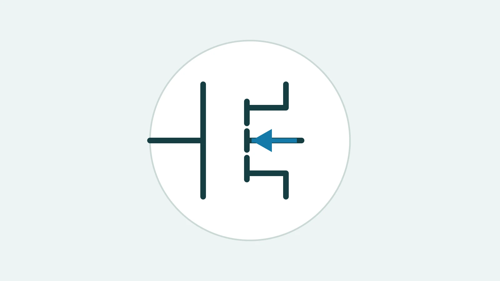
A MOSFET symbol gives channel and sometimes mode clues, but it does not establish package pin order. Verify the exact device, symbol library and footprint against controlled manufacturer datasheets and package documentation before release.
For the broader language of circuit drawings, see schematic symbols. For a MOSFET, the practical decision is narrower: can the team trace each intended electrical terminal from the schematic, through the library and PCB, to an evidenced physical connection?
First decision: what does the symbol actually tell you?
Start with the gate, drain, source and, if shown separately, body or bulk. The gate is insulated from the channel in the ordinary MOSFET model. Its controlling voltage is gate-to-source voltage, VGS—not gate voltage measured to ground unless the source happens to be at ground.
A symbol may suggest two independent properties:
- Channel type: N-channel or P-channel.
- Operating mode: enhancement or depletion.
An N-channel device generally needs a more positive gate relative to its source to increase channel conduction. A P-channel device generally needs a more negative gate relative to its source. These statements describe gate control, not a universal drain-current direction for every device or operating condition.
For an enhancement-mode device, the channel is not established at VGS = 0 under the normal operating model. For a depletion-mode device, a channel exists at VGS = 0 and an appropriate gate-to-source voltage can reduce its conduction. “Not established” does not mean zero leakage, nor does it eliminate a possible body-diode path.
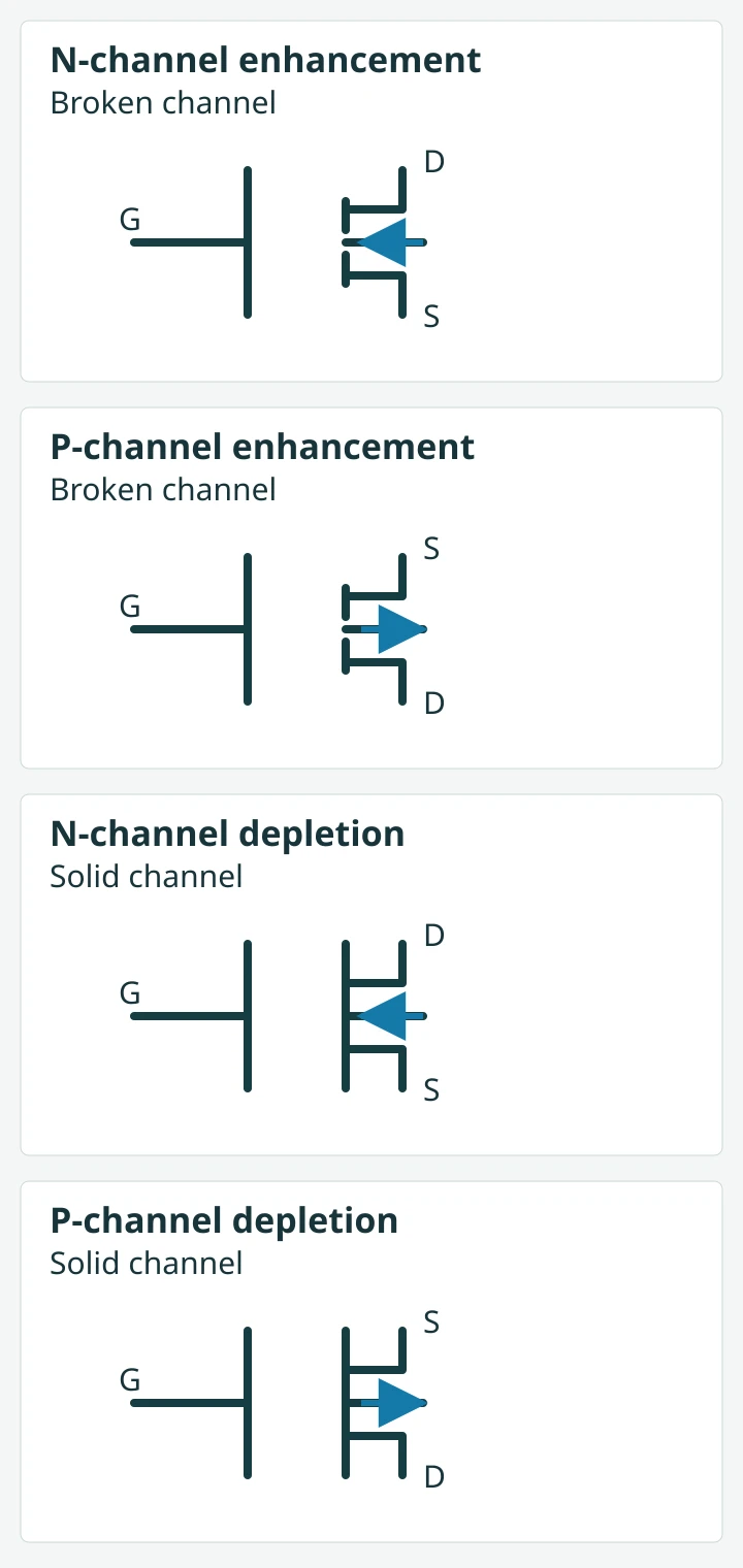
Scope: the matrix illustrates symbol concepts, not the identity or pinout of a particular part.
A broken channel line is often used for enhancement mode and a solid channel line for depletion mode. That is a convention-dependent clue, not proof: a library may use another style or omit the distinction. Check the manufacturer’s device description and electrical characteristics.
Read the arrow according to its job
Do not apply one universal “arrow in” or “arrow out” mnemonic to every MOSFET symbol. First determine where the arrow is drawn and what it represents.
Body or bulk arrow
In a common four-terminal convention, the arrow represents the body-to-channel junction and points from P-type material toward N-type material. Thus, for an N-channel device with a P-type body, it points toward the N-type channel. For a P-channel device with an N-type body, it points away from the P-type channel toward the body.
The arrow identifies a junction convention; it is not a command that load current must always flow in the arrow’s direction.
Simplified source-leg arrow
Some three-terminal symbols put an arrow on the source leg instead. In one common source-leg convention, the N-channel arrow points outward from the device and the P-channel arrow inward. That apparent direction can oppose the corresponding body-arrow description because the arrow’s location and reference are different.
Treat a source-leg arrow as meaningful only within the drawing or library convention that defines it. If the symbol is unfamiliar, consult its library documentation and the device datasheet rather than guessing from the arrow alone.
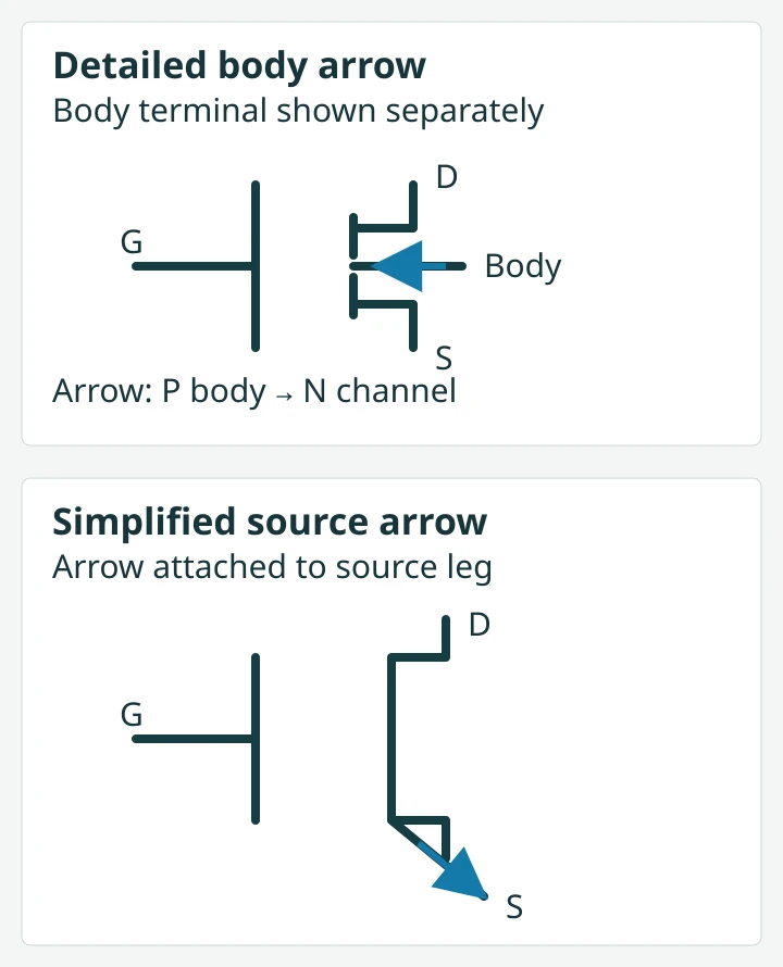
Scope: this comparison concerns arrow conventions; it does not establish a package view or physical pin order.
Check the body-diode assumption
For a conventional three-terminal silicon power MOSFET with its body tied to its source, the structure normally includes a body-to-drain diode:
- In an N-channel device, the diode is normally shown with its anode at source and cathode at drain.
- In a P-channel device, it is normally shown with its anode at drain and cathode at source.
A suitable voltage can forward-bias that diode even when the gate is not establishing a channel. Conversely, a sufficiently enhanced channel can support current in either direction under appropriate conditions. The diode symbol alone is therefore not a complete operating or protection analysis.
Do not extend this construction automatically to every MOSFET, integrated switch, technology or four-terminal device. Check the specific device’s internal diagram, ratings and operating conditions.
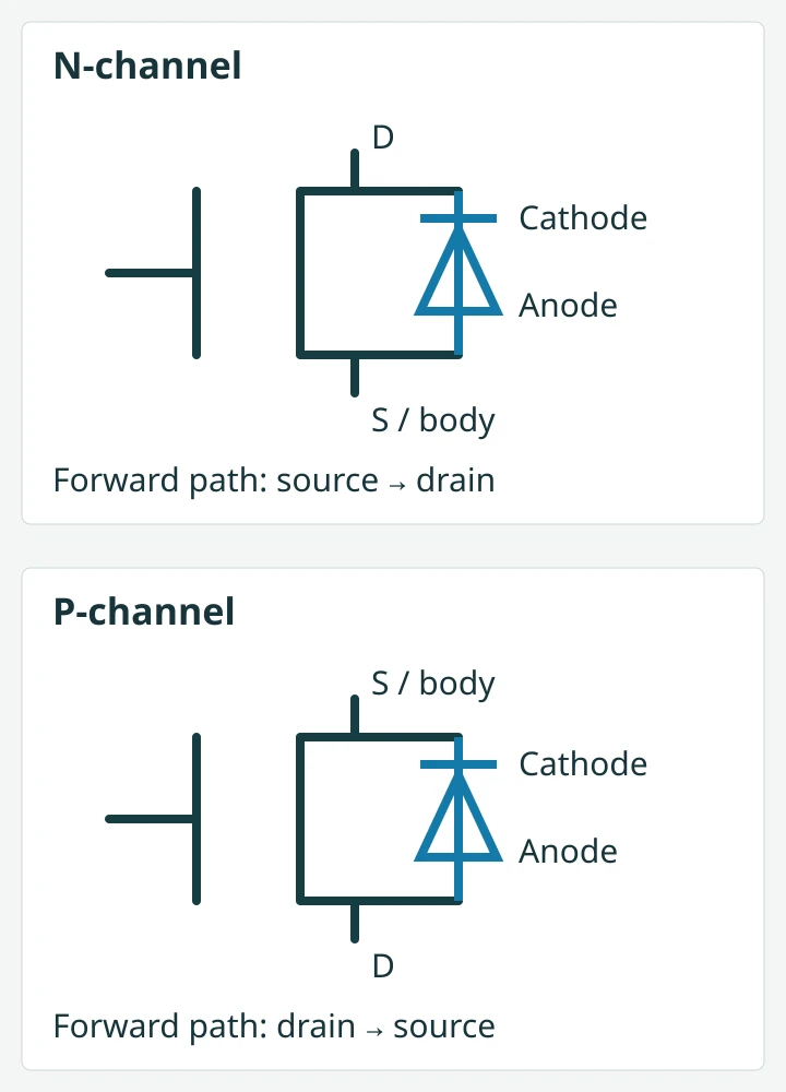
Scope: the diode orientations shown apply to the stated body-tied-to-source construction, not to all transistor structures.
The release decision: prove the mapping, not the picture
A schematic symbol is a logical interface. A footprint is a physical interface. Their connection depends on library data that associates symbol terminals with footprint pads. A plausible drawing can hide a wrong association.
Do not infer channel polarity, exact part identity or terminal order from a footprint outline, package shape, mounting tab, or resemblance to another transistor. Even if a device family has a familiar arrangement, the controlled evidence must apply to the exact manufacturer part number and package being released.
Trace the chain:
- Identify the intended gate, drain and source in the design.
- Inspect the actual symbol library terminal names and terminal numbers.
- Obtain the manufacturer’s applicable package drawing, with its viewing orientation and terminal identification understood.
- Inspect the actual footprint pad numbers and geometry, including any tab or exposed copper feature.
- Compare those records with the PCB layout and assembly drawing. Resolve every discrepancy before release.
A front view, rear view and footprint viewed from the PCB side can look deceptively similar while reversing the apparent left-to-right order. Record the orientation explicitly; do not rely on the page image alone.
For the broader handoff between circuit design and board layout, see the schematic-to-PCB workflow checklist.
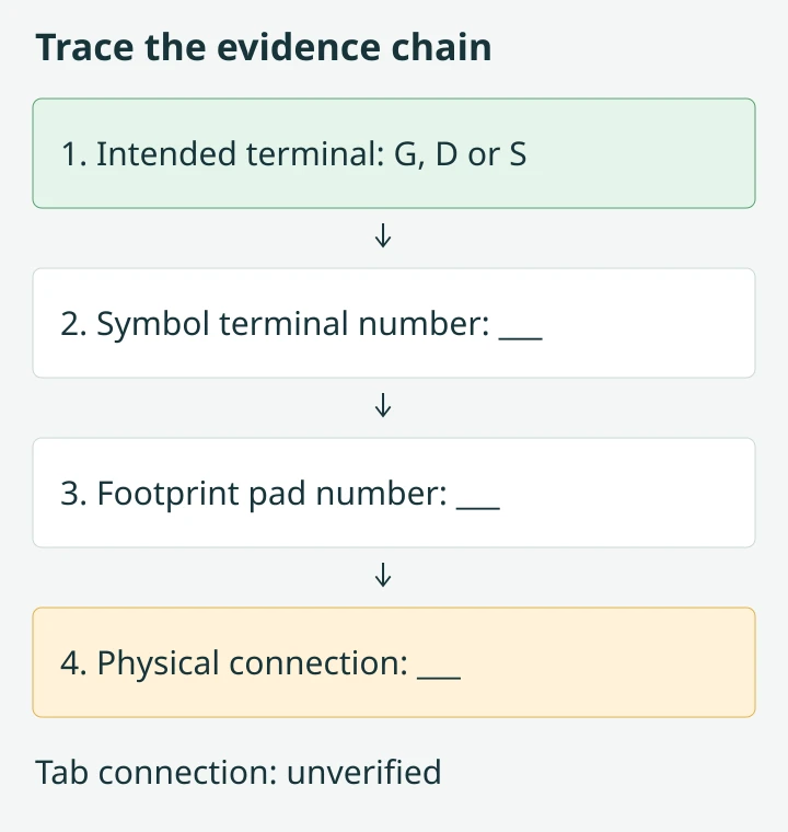
Scope: the chain is a verification aid. It does not by itself establish numeric pin assignments or a tab connection for FQP30N06L.
The table below is a fictional review example, not the pinout of FQP30N06L or any other actual device. Assume its hypothetical manufacturer drawing uses a stated top view and identifies leads 1, 2 and 3 as gate, drain and source, respectively. The library and PCB entries are also invented; no actual manufacturer document or board was checked for this example.
| Intended terminal | Fictional symbol pin | Assumed manufacturer lead and view | Fictional footprint pad and PCB net | Review result |
|---|---|---|---|---|
| Gate | 1, on GATE_CTRL |
Lead 1, gate; top view | Pad 1, GATE_CTRL |
Entries agree within this fictional example. |
| Drain | 2, on DRAIN_LOAD |
Lead 2, drain; top view | Pad 2, SOURCE_RETURN |
Hold: the PCB net conflicts with the intended drain net. |
| Source | 3, on SOURCE_RETURN |
Lead 3, source; top view | Pad 3, SOURCE_RETURN |
Entries agree within this fictional example. |
| Tab or exposed pad, if present | Not assumed | Connection not established in this example | Physical feature and copper connection not established | Hold until the applicable drawing and layout resolve the feature. |
For the fictional drain mismatch, trace the actual design data to find the cause, correct the responsible library or layout, and regenerate the controlled outputs before reviewing again. Do not merely rename a net to make the records appear consistent. Agreement in this table still does not prove physical fit, the drawing view, assembly orientation or electrical suitability.
Use a separate record for each real device and library combination. Record the exact manufacturer part number, document revision, drawing view, symbol pin numbers, footprint pads and copper connections; add separately relevant body, exposed-pad or tab rows. If the applicable manufacturer document does not explicitly establish a needed package-to-signal or tab connection, request a controlled drawing or written clarification. Hold the mapping open rather than filling the gap from habit.
ERC and DRC are necessary but insufficient. Electrical rule checking can validate rules against the symbol and netlist it was given; design rule checking can validate layout constraints against the PCB data it was given. Neither can prove that a consistently numbered—but incorrect—library mapping matches the real device.
Bounded example: FQP30N06L Rev. C1
The following values are limited to the reviewed FQP30N06L manufacturer datasheet, Rev. C1, at case temperature TC = 25 °C unless otherwise noted. They illustrate why symbol identification and gate-drive selection are separate checks; they are not a general design recommendation. Confirm the applicable current documentation for the exact ordering variant before use.
The document identifies an N-channel device and specifies:
- Gate threshold voltage: 1.0 to 2.5 V, measured at VDS = VGS and ID = 250 µA.
- Maximum RDS(on): 35 mΩ at VGS = 10 V and ID = 16 A.
- Maximum RDS(on): 45 mΩ at VGS = 5 V and ID = 16 A.
Threshold is a measurement at a very small test current. It is not the gate drive required for low-resistance operation. For a design, compare the available gate-to-source drive and its tolerances with the relevant datasheet conditions, then assess losses, temperature, transients and the rest of the operating envelope.
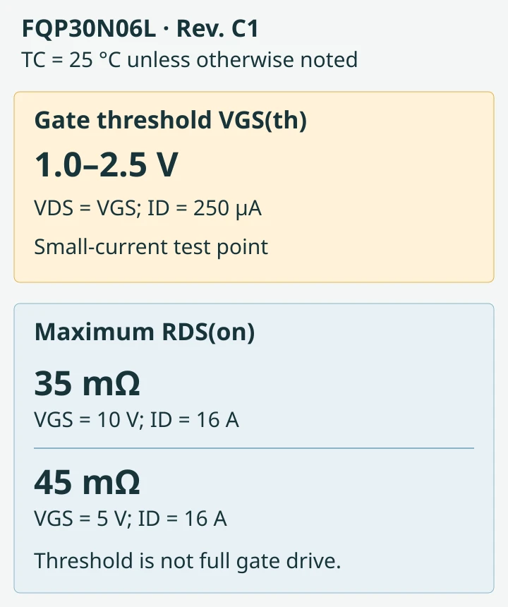
Scope: the illustration contrasts test conditions; it is not a gate-drive recommendation.
The reviewed document depicts G, D and S, but does not explicitly establish numeric package-to-signal mapping or the tab connection for this verification. Do not assign physical pin or footprint pad numbers—or assume a tab connection—from this example. Obtain adequate controlled package evidence for the exact ordering variant before approving its library mapping.
Symbol-to-part release checklist
Before releasing the design package, the designer or library owner should record and review the following:
- Identity: exact manufacturer part number, ordering suffix and package; approved alternatives are individually checked rather than presumed equivalent.
- Source control: manufacturer document title, revision and applicable package drawing; viewing orientation and any manufacturer clarification are recorded.
- Electrical intent: N/P channel, enhancement/depletion mode, gate-drive reference and operating requirements checked against the exact device.
- Library mapping: symbol terminal names and numbers traced to footprint pads using the evidence table; tab or exposed-pad treatment resolved where applicable.
- Design files: released schematic and netlist, native or versioned symbol and footprint libraries, PCB layout, and fabrication outputs including copper and drill data.
- Assembly files: controlled BOM, assembly drawing, placement/centroid data, reference designators, orientation convention and any special handling or inspection instructions.
- Approval: the designated drawing owner approves the mapping, package view, assembly orientation and revision set; unresolved evidence is a release hold.
- First article: requested checks and acceptance criteria are written into the build package, with responsibility for review and disposition named.
For first-article review, request verification of the fitted part and available marking against the approved records, placement orientation against the controlled drawing, and the intended terminal-to-board connections against the approved mapping. Specify solder-joint or exposed-feature inspection as applicable, and any continuity, shorts or powered checks with safe conditions and acceptance limits. A marking or inspection result alone does not prove the semiconductor’s full performance.
If another part is proposed, use the component substitution approval checklist to document the change and its required approvals. The PCB assembly inspection report checklist can help record the agreed inspection scope and exceptions.
For an assembly quotation, provide the controlled BOM, design files, verified mapping and any open questions through the quote page. The PCB assembly quote guide explains the information needed to compare supplier responses.
Keep responsibilities separate
The designer and library owner own the design intent and the correctness of the symbol-to-footprint mapping. They select the part, resolve ambiguity, control revisions and approve the drawing.
The part manufacturer supplies the applicable device specifications, package information and, when needed, clarification. Its documentation supports the mapping; it does not automatically approve the customer’s library or board.
The PCB assembler builds and inspects to the agreed, controlled package and reports discrepancies. Assembly inspection is not a substitute for the design owner’s terminal-mapping approval.
The system qualification owner establishes and performs the product-level verification appropriate to the application, including electrical and thermal limits, fault behavior and acceptance criteria. Passing a manufacturing check does not by itself qualify the system.
Frequently asked questions
Can an arrow alone identify every MOSFET?
No. Its meaning depends on whether it is a body arrow, a source-leg arrow or another library representation. Use the symbol convention and verify the device against its manufacturer documentation.
Does a dashed channel prove enhancement mode?
Not universally. A dashed or broken line is a common enhancement-mode clue, while a solid line is often used for depletion mode. A drawing may use another convention or omit the distinction.
Can I use gate threshold as the required drive voltage?
No. Threshold is specified at a particular test condition and does not establish low on-resistance. Check RDS(on) at an applicable VGS and current, then evaluate the full operating conditions.
Will ERC or DRC catch swapped MOSFET terminals?
Not reliably. Both checks can pass if the schematic and layout are internally consistent but the library’s symbol-to-physical-part mapping is wrong.
What if the package document does not explicitly identify a tab or pin connection?
Leave it unverified and obtain applicable controlled manufacturer evidence or clarification. Do not infer the connection from package appearance or another part’s pinout.