
When a via or component pad fails a fabrication DFM check for insufficient annular ring, the discrepancy usually starts with an unstated reference boundary: did the layout engineer subtract the finished hole diameter from the pad diameter while the fabricator's CAM rule subtracted the compensated production drill diameter? Because plated through-holes are drilled larger than their finished opening to accommodate electroless copper, electrolytic barrel plating, and surface finish, those two equations yield different radial ring widths on the exact same CAD padstack.
Resolving annular ring margin before release requires three engineering steps: locking the hole-reference boundary with the fabricator, evaluating inner layers separately from outer layers to account for lamination registration shift, and checking that any pad enlargement does not violate adjacent trace or plane clearances. For broader pre-release verification across trace/space, aspect ratio, and netlist checks, see our PCB DFM review guide.
1. Tool Reference vs. Finished-Hole Reference: Why Two Correct Equations Disagree
An annular ring is the width of copper land remaining around a drilled hole. On an ideal concentric padstack, the nominal radial width is half the diameter difference between the copper pad and the hole reference:
In PCB design and inspection, however, Dref is defined in two distinct ways depending on whether you are running a pre-production CAM design rule check or inspecting a finished board:
- Tool-Size Design Reference (Dref = Dtool): Many bare-board fabricators evaluate incoming CAD annular ring rules against the production drill bit diameter (Dtool) rather than the finished plated hole size. As documented in fabricators' published drill-classification and design rules, the drill bit physically cuts away the copper foil on both outer and inner layers. If a 0.30 mm finished via is drilled with a 0.40 mm production tool inside a 0.60 mm pad, the nominal copper ring left around the drill bit is (0.60 - 0.40)/2 = 0.10 mm, not the (0.60 - 0.30)/2 = 0.15 mm displayed in a CAD tool set to finished hole size.
- Finished Inspection Reference (External vs. Internal Lands): During final quality inspection (such as metallographic cross-sectioning or optical inspection under IPC-6012 / IPC-A-600), external annular ring is measured from the inside surface of the plated hole wall (or edge of the hole on non-plated holes) to the outer edge of the surface pad, whereas internal annular ring is measured from the edge of the drilled hole wall to the outer edge of the internal copper land. Crucially, barrel copper plated inside the hole wall adds axial strength and electrical continuity, but plating does not restore internal capture-pad copper that was already severed by the drill bit.
| Dimension in the Padstack | Physical Meaning in Fabrication | Typical Impact on Annular Ring Calculation |
|---|---|---|
| Finished Hole Size (DFHS) | Clear inner diameter after barrel copper plating and surface finish (HASL, ENIG, etc.) | Controls component pin fit or via opening; overstates available drill-to-pad margin if used directly in inner-layer ring equations |
| Production Drill Diameter (Dtool) | Actual mechanical drill bit or laser aperture diameter used by CAM to achieve DFHS | Directly determines how much copper land is removed when the hole is drilled through the stackup |
| Released Pad Diameter (Dpad) | Copper land diameter on the specific layer in Gerber / ODB++ / IPC-2581 artwork | Outer pads, inner signal pads, and plane thermal-relief pads may have different diameters on the same hole |
| Finished Etched Pad (Dpad,min) | Actual copper diameter remaining after outer/inner imaging and chemical etching | Lateral etch undercut reduces the effective land radius available to absorb drill offset |
2. Why Inner Layers Fail First: Lamination Movement and Registration Stackup
A padstack that passes comfortably on Layer 1 and Layer N frequently fails on internal signal layers (L2, L3, etc.). Outer layers are imaged after mechanical through-hole drilling, allowing direct optical alignment (LDI) to fiducials drilled in the same setup. Inner layers, by contrast, are etched onto individual cores before lamination and drilling, exposing them to three cumulative positional error sources:
- Lamination Scale and Non-Linear Material Movement: During high-temperature, high-pressure lamination cycles, prepreg resin flows and glass-reinforced cores expand, contract, and relax non-uniformly along the warp and weft directions of the glass cloth. Even with core-specific scale compensation factors applied in CAM, residual dimensional variance remains.
- Layer-to-Layer Alignment Tolerance: Optical or X-ray registration aligns multiple etched cores prior to pressing, introducing core-to-core alignment tolerances (a tolerance that major fabricators publish in their design rules).
- Mechanical Drill Runout (Wander): As a small mechanical drill bit penetrates a thick multilayer board or high-glass-content laminate, glass bundles deflect the bit tip laterally, increasing positional error at deeper internal layers.
To evaluate whether a padstack can survive fabrication without unintended breakout, separate dimensional loss (pad etch reduction and tool enlargement) from relative radial center offset (Δ r):
Note that Δ r\max represents the combined radial center-to-center offset between the etched pad and the drilled hole on that specific layer. If a fabricator provides a consolidated registration allowance that already accounts for core movement and drill accuracy, do not subtract a second separate drill tolerance on top of it.
Worked Layer-by-Layer Tolerance Stackup (L1 vs. L2 vs. L4)
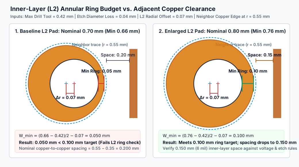
Consider a 4-layer board reviewed against an illustrative project minimum of 0.10 mm remaining radial ring. The outer pads (L1, L4) are designed at 0.80 mm nominal diameter, while the inner signal pad (L2) was reduced to 0.70 mm to route an adjacent trace:
| Layer & Scenario | Nominal Pad (Dpad) | Etch Loss (Δ Detch) | Min Pad (Dpad,min) | Max Tool (Dtool,max) | Radial Offset (Δ r\max) | Nominal Ring (Wnom) | Worst-Case Min Ring (W\min) | Engineering Disposition |
|---|---|---|---|---|---|---|---|---|
| L1 Outer (Baseline) | 0.80 mm | 0.04 mm | 0.76 mm | 0.42 mm | 0.05 mm | 0.200 mm | 0.120 mm | Passes 0.100 mm target (+0.020 mm margin) |
| L4 Outer (Baseline) | 0.80 mm | 0.04 mm | 0.76 mm | 0.42 mm | 0.06 mm | 0.200 mm | 0.110 mm | Passes 0.100 mm target (+0.010 mm margin) |
| L2 Inner (Baseline) | 0.70 mm | 0.04 mm | 0.66 mm | 0.42 mm | 0.07 mm | 0.150 mm | 0.050 mm | Fails 0.100 mm target (−0.050 mm shortfall) |
| L2 Option A (Enlarge Pad) | 0.80 mm | 0.04 mm | 0.76 mm | 0.42 mm | 0.07 mm | 0.200 mm | 0.100 mm | Meets 0.100 mm target; check neighbor spacing |
| L2 Option B (Smaller Tool) | 0.70 mm | 0.04 mm | 0.66 mm | 0.32 mm | 0.07 mm | 0.200 mm | 0.100 mm | Meets 0.100 mm target; check hole aspect ratio / fit |
(Full editable dataset: layer-margin-example.csv and change-tradeoffs.csv.)
Inspecting only a top-layer CAD screenshot shows a 0.200 mm nominal ring and a 0.120 mm worst-case outer ring, completely hiding the 0.050 mm inner-layer shortfall on L2.
Evaluating the Tradeoff: Pad Enlargement vs. Adjacent Copper Spacing
When L2 fails the ring budget, neither Option A nor Option B can be approved in isolation:
- Consequence of Option A (Enlarging L2 Pad from 0.70 mm to 0.80 mm): Suppose an adjacent L2 signal trace edge sits at a fixed radial distance of r = 0.55 mm from the hole center. Increasing the nominal L2 pad diameter from 0.70 mm (rpad = 0.35 mm) to 0.80 mm (rpad = 0.40 mm) reduces the nominal pad-to-trace edge clearance from 0.55 - 0.35 = 0.20 mm down to 0.55 - 0.40 = 0.15 mm. Before approving the pad increase, confirm that 0.15 mm (6 mil) satisfies your inner-layer copper weight etch rules, dielectric breakdown spacing, and crosstalk budget.
- Consequence of Option B (Reducing Max Tool from 0.42 mm to 0.32 mm): If the hole is an interconnect via, dropping the drill size increases the hole aspect ratio (board thickness divided by drill diameter), which can push a thick board beyond standard plating throwing power. If the hole is a component PTH, reducing the drill changes the finished opening and can prevent component lead insertion (covered in detail in our finished hole size and drill tolerance guide).
3. Tangency, Breakout, Teardrops, and Non-Functional Pads (NFPs)
When drill offset equals the available radial copper margin, the hole edge touches the outer boundary of the pad (tangency, W\min = 0). If the offset exceeds that margin, the hole extends outside the pad boundary (annular ring breakout, W\min < 0).
Whether tangency or limited breakout is acceptable depends on the governing contractual standard and product class (see IPC Class 1 vs. Class 2 vs. Class 3 criteria):
- High-Reliability / Class 3 Builds: Typically require a continuous external and internal annular ring (e.g., ≥ 0.050 mm external and ≥ 0.025 mm internal minimum copper land) with no breakout permitted, ensuring 360° structural anchoring of the plated barrel under thermal cycling.
- Dedicated-Service / Class 2 Builds: Commonly permit limited 90° breakout on vias or lands provided the conductor-to-land junction is never reduced below the minimum allowed trace width and the breakout does not violate minimum electrical spacing to adjacent nets.
- Why Teardrops Are Essential at Trace Entry: Even where 90° breakout is contractually allowed, breakout occurring at the exact angle where a narrow trace joins the pad can sever the circuit or create a high-resistance neck. Adding teardrop fillets tapers the copper transition at the trace-to-pad junction, providing extra radial copper along the connected vector without enlarging the entire circular pad across tight BGA escape channels.
- Non-Functional Pads (NFPs) on Inner Layers: On high-layer-count boards, vias often pass through internal signal layers where they have no electrical connection. Removing unconnected inner-layer NFPs eliminates the risk of inner-layer breakout on unconnected layers, reduces parasitic via capacitance on high-speed SerDes channels, and reduces drill wear—provided the fabricator confirms that NFP removal does not destabilize local copper balance or hole-wall desmear quality.
4. Reviewing Padstacks Across Special Geometries and Via Structures
A single circular equation does not cover every feature on a modern multilayer PCB. During pre-release review, audit these four geometry cases explicitly:
- Plated Slots and Oblong Pads: A routed plated slot has straight sides and semi-circular ends. Evaluate annular ring along the full contour—both laterally (Wpad - Wslot) and longitudinally (Lpad - Lslot)—accounting for mechanical routing cutter tolerances rather than standard twist-drill tolerances.
- Laser Microvias and Stacked/Staggered HDI Structures: In sequential build-up HDI stacks, a laser microvia (typically 0.05--0.125 mm diameter) lands on an internal target pad rather than passing through it. The critical check is both the top capture pad ring and the bottom target land containment so the laser beam never ablates into the underlying dielectric outside the target copper pad.
- Via-in-Pad Plated Over (VIPPO): When vias are placed directly inside fine-pitch BGA or QFN SMD pads, verify the resin/copper fill and planarized cap specification using the via-filling material guide alongside the drill-to-pad margin.
- Anti-Pad Clearances on Internal Planes: When you enlarge a via's internal capture pad on L2, verify whether the anti-pad opening on adjacent power/ground planes (L3, L5) must also expand to prevent plane-to-barrel shorts during drill wander.
5. Evaluating Supplier DFM Feedback and Submitting the Release Package
When a fabricator flags an annular ring exception during CAM preflight, require a specific, bounded engineering query (EQ) rather than a vague request to "accept CAM optimization":
| Fabricator EQ Response Style | What It Tells Engineering | Required Follow-Up Before Sign-Off |
|---|---|---|
| "Annular ring is tight; please confirm we can modify working files as needed." | Unbounded request; does not state which layers, nets, hole sizes, or clearances will change | Reject blanket permission. Ask for the exact drill tool table, affected layer list, and marked before/after Gerber overlay |
| "Via group D04 (0.25 mm FHS / 0.35 mm tool) has 0.05 mm nominal ring on L2/L5. Propose enlarging L2/L5 connected pads from 0.45 mm to 0.50 mm and removing unconnected NFPs; minimum L2 trace-to-pad space becomes 0.11 mm (see attached overlay CAM-B1)." | Actionable, traceable engineering proposal with explicit clearance impact | Verify that 0.11 mm spacing and NFP removal meet electrical/impedance rules; approve CAM-B1 in writing and update master CAD padstack for future builds |
What to Include in Your PCB Fabrication RFQ
To eliminate annular ring holds during CAM engineering, include the following in your PCB manufacturing release package:
- Synchronized Artwork and Drill Files: Gerber (
RS-274X/Gerber X2),ODB++, orIPC-2581data with an explicit drill table stating whether nominal drill values represent Finished Hole Size (FHS) or uncompensated tool diameters. - Governing Acceptance Standard and Class: Specify the exact bare-board standard and class on the master drawing (e.g., IPC-6012 Class 2 or IPC-6012 Class 3, plus whether 90° via breakout is permitted or prohibited).
- Inner-Layer NFP and Teardrop Policy: State clearly in the fabrication notes whether CAM is authorized to remove non-functional internal pads or add teardrops on inner signal layers, and mark any RF/high-speed nets where pad geometry is frozen for impedance control.
- Downloadable Review Templates: Use layer-margin-example.csv and change-tradeoffs.csv (notes) to document layer-specific pad/tool budgets across critical via families.
HILPCB manufactures multilayer PCBs up to 64 layers and sequential HDI PCBs using optical and X-ray layer-to-layer registration systems holding alignment typically within ±15–25 µm, mechanical drills down to 0.15 mm, and laser microvias down to 0.05–0.10 mm. Upload your Gerber or ODB++ package when you request a quote so our CAM engineers can verify inner-layer annular ring margins, pad-to-trace clearances, and drill compensation against your target IPC class before production starts.
Frequently Asked Questions
Why is my fabricator's annular ring calculation smaller than what my CAD software shows?
Most EDA tools calculate annular ring by subtracting the finished hole diameter from the pad diameter, whereas fabricator CAM rules subtract the compensated production drill bit diameter. Because plated through-holes are drilled 0.10--0.15 mm larger than the finished hole to allow for copper plating and surface finish, the actual copper ring remaining around the drill bit is 0.05--0.075 mm narrower per side than the nominal finished-hole calculation.
Does copper plating inside the hole barrel increase the inner-layer annular ring?
No. On internal layers, the mechanical drill bit punches directly through the etched inner-layer copper foil. Subsequent electroless and electrolytic copper plating deposits copper onto the inner wall of the hole barrel to form the vertical interconnect, but it does not restore horizontal capture-pad width outside the drilled boundary.
What is the difference between tangency and annular ring breakout?
Tangency occurs when the outer perimeter of the drilled hole touches the outer edge of the copper pad (0 mm minimum remaining width at one point without extending outside the pad contour). Breakout occurs when the hole extends past the pad edge (W\min < 0). While IPC-6012 Class 2 typically allows up to 90° of breakout on vias provided trace junctions remain intact, Class 3 generally requires a continuous minimum annular ring with zero breakout.
When should I add teardrops instead of enlarging the entire via pad?
Use teardrops when routing density (such as under a 0.8 mm or 0.65 mm pitch BGA) prevents enlarging the circular pad diameter without violating trace-to-pad clearance rules. Teardrops reinforce the copper specifically along the trace-entry vector—preventing drill offset from severing the trace-to-pad neck—while keeping the perpendicular sides of the pad within the channel clearance budget.