

A via filling material guide is a decision framework for selecting the hole-protection structure, fill system, lamination sequence, cap plating, and acceptance evidence—not merely choosing conductive or non-conductive paste. It is most useful before stackup release, when the PCB designer and fabricator can still align via function, material construction, assembly risk, and test methods.
Key Takeaways
- Start with the reason a hole needs protection: solder control, via-in-pad planarity, contamination sealing, sequential lamination, thermal transfer, or another defined objective.
- Use IPC-4761 terminology to distinguish tented, plugged, filled, covered, and filled-and-capped structures.
- A non-conductive resin-filled via remains electrically conductive through its copper-plated barrel; the resin is not the signal path.
- Via-in-pad normally requires complete filling, planarization, and metal capping when the pad must become a flat solderable surface.
- Material names, nominal Dk/Df, data rate, layer count, and Tg are not stand-alone selection rules. The released construction, test method, process window, channel budget, and reliability environment matter.
- Specify how each critical feature will be accepted: microsection, cap-plating measurement, planarity inspection, impedance coupon, thermal cycling, assembly trial, or another controlled method.
Table of Contents
- What Does Via Filling Actually Specify?
- Map IPC-4761 Via Protection Types
- Use a Function-First Via Filling Decision Tree
- How Should Via-in-Pad Be Filled and Capped?
- Choose Fill Material by Function and Evidence
- Coordinate Via Filling with Stackup and Lamination
- Build a Controlled Material Identity Record
- Select Prepreg, Core, and Glass Construction
- Qualify Hybrid Stackups and Surface Finish
- Control Impedance, Warpage, and Reliability
- Diagnose Via-Filling Failure Modes
- Qualify Substitute Materials
- Plan Cost Without Cutting Evidence
- Via Filling and Stackup RFQ Checklist
- Reference Standards and Responsibility Boundaries
- How HILPCB Supports Stackup Review
- Frequently Asked Questions
What Does Via Filling Actually Specify?
The phrase “filled via” is often used too loosely. A drawing may call a hole filled even though the intended result is only a solder-mask plug, or it may request “VIPPO” without defining which holes, which surfaces, the cap, the finish, or the acceptance criteria. Those gaps force CAM and process engineering to infer design intent.
Q1: What problem does the via need to solve?
First identify the functional objective. Different objectives can require different structures even when the hole diameter is identical.
| Objective | Typical concern | Structure to evaluate | Evidence to request |
|---|---|---|---|
| Prevent solder wicking | Solder drains through an open via during reflow | Tenting, plugging, filling, or relocating the via | Assembly trial, visual/X-ray evidence, solder-joint acceptance |
| Put an SMT pad over a via | Pad must be flat and solderable | Filled, planarized, metal-capped via | Surface inspection, cap-plating measurement, microsection |
| Seal process chemistry or contamination path | Residue or liquid can remain in a cavity | Filled or otherwise protected via | Process review, sectioning, cleanliness evidence where applicable |
| Build stacked structures | A later via or layer depends on a stable underlying surface | Filled-and-capped structure compatible with the build sequence | Sequential-lamination traveler, registration and microsection evidence |
| Create a thermal path | Heat must reach planes, a spreader, or metal structure | Plated via array, filled via, copper coin, or another thermal architecture | Thermal model and temperature-rise test at defined boundary conditions |
| Protect an unused/open hole | Environmental or coating requirement | Tented, covered, plugged, or filled structure | Coverage inspection and application-specific qualification |
This first question prevents a common mistake: paying for a complex fill when tenting is sufficient, or specifying a low-cost plug where a solderable via-in-pad surface actually needs complete fill and cap plating.
Q2: Which hole population is controlled?
The fabrication package must identify exactly which holes receive which process. Do not rely on diameter alone when component holes, mechanical holes, test holes, and vias share sizes. Provide a dedicated via-fill layer or unambiguous drill attributes, a legend for the protection types, and a drawing note linked to the correct drill span.
For HDI, distinguish laser microvias, mechanically drilled blind vias, buried vias, and through vias. Their fill mechanism and position in the lamination flow can differ. “Fill all vias” is not a safe instruction unless every hole has been reviewed for assembly, venting, plating, and cost.
Map IPC-4761 Via Protection Types
IPC-4761 provides a shared vocabulary for protecting printed-board via structures. The lettered single-side and double-side variants should be confirmed against the edition and drawing convention used by the customer and fabricator.
| IPC-4761 family | Basic structure | What it does not automatically guarantee | Typical decision use |
|---|---|---|---|
| Type I: tented | Solder mask spans the opening | Complete sealing, a flat pad, or a filled barrel | Low-cost protection where mask geometry and process capability allow |
| Type II: tented and covered | Tented opening receives an additional covering | Solid internal fill or metal cap | Extra mask protection without a filled barrel |
| Type III: plugged | Material plugs one or both ends for a specified depth | Complete barrel fill or a planar solderable surface | Solder/control objectives that do not require full filling |
| Type IV: plugged and covered | Plug is supplemented by covering material | Complete fill, cap plating, or via-in-pad planarity | More robust mask-side protection |
| Type V: filled | Barrel is filled with specified material | Metal capping or a solderable pad | Sealed/solid hole where cap plating is not required |
| Type VI: filled and covered | Filled hole receives covering material | Metal cap or pad restoration | Filled structure protected by mask/cover material |
| Type VII: filled and capped | Filled hole is planarized and metallized over | Suitability for every stack, pitch, reliability class, or assembly profile | Via-in-pad and structures that need a flat metal surface |
Q3: Is the request for filling, plugging, or covering?
These terms are not interchangeable. Plugging controls material at the ends of a hole; filling controls the barrel volume; covering controls a surface layer; capping adds metallization over a filled, prepared surface. A board can look closed from the outside yet retain an internal cavity that behaves differently during cure, plating, or reflow.
The drawing should use the protection type and a plain-language result. For example: “Specified PTH vias: IPC-4761 Type VII, resin filled, planarized, and copper capped; apply to holes on VIA_FILL layer.” Then state the required acceptance document rather than assuming the standard name alone settles sampling and limits.
Use a Function-First Via Filling Decision Tree
The fill material is not the first branch. Use this sequence before asking for a paste brand or conductivity value:
- Does the hole need to be sealed? If not, compare leaving it open, tenting, or relocation.
- Will solder paste or a component termination sit over the hole? If yes, define the required planarity and solderable metal surface.
- Does the finished feature require metal capping? Via-in-pad commonly does; an internal or masked hole may not.
- Is the via part of a sequential-lamination or stacked-microvia structure? If yes, the fill and cap become part of the next build stage.
- Is thermal transfer a quantified requirement? If yes, compare the complete thermal network rather than assuming conductive paste solves it.
- What are the hole diameter, finished diameter, depth, aspect ratio, copper thickness, and board construction? These determine feasible filling and inspection methods.
- How will the result be accepted? Define section locations, surface inspection, cap-plating measurement, allowed anomalies, sampling, and reporting.
Q4: When is Type VII appropriate?
Type VII is a strong candidate when an SMT pad must cover the via, when another conductive feature depends on a planar metal surface, or when the selected HDI construction requires a filled-and-capped foundation. It is not a generic upgrade for every via. It adds dedicated drilling/plating coordination, filling, curing, planarization, cap plating, inspection, and yield risk.
One fabricator’s published process is a useful example of why supplier capability data must remain supplier-specific: a Type VII resin route defines particular through-hole ranges, board thicknesses, process steps, and data rules. Those numbers describe that production offering, not universal IPC limits. HILPCB should therefore review the actual stackup and hole table before the designer freezes a capability around another manufacturer’s published range.
How Should Via-in-Pad Be Filled and Capped?
Via-in-pad removes dog-bone routing space by placing the interconnect directly in an SMT pad. The benefit is density and a shorter transition; the manufacturing price is that the via becomes part of the solder-joint interface.
Q5: What makes a via-in-pad surface assembly-ready?
A production-ready via-in-pad feature normally needs four controlled outcomes:
- The plated barrel provides the intended interlayer connection.
- The fill supports the surface and does not leave an unacceptable void or recession.
- Planarization removes protrusion without damaging the surrounding pad.
- Cap plating restores a continuous, flat metal surface compatible with the final finish and assembly process.
Leaving a via open beneath paste can draw solder away from the joint. A shallow mask plug may close the visible opening but is not equivalent to a solid, capped pad. A recessed or crowned cap can change paste volume and component stand-off; weak adhesion or thin cap copper can crack during later thermal exposure.
For BGAs, QFNs, LGAs, thermal pads, and fine-pitch passives, release the component land pattern, via drill/finished size, pad size, copper weight, paste aperture, solder-mask definition, assembly profile, and inspection plan together. The fabricator can control the bare-board structure, but only the assembly trial can prove the joint behavior for the selected package, paste, stencil, and reflow window.
Q6: Do all thermal-pad vias need conductive fill?
No. Thermal performance depends on the complete path: component junction, package exposed pad, solder layer, copper lands and planes, plated barrels, fill if used, board thickness, heat spreader, airflow, and ambient condition. The copper barrel and connected copper usually dominate the electrical connection in a non-conductive resin-filled via.
An array of appropriately plated vias may outperform an expensive paste choice when the real bottleneck is plane area, interface resistance, airflow, or heat-sink contact. Conductive fill can be evaluated when it produces a modeled and measurable benefit, but its thermal conductivity value alone is not proof of lower junction temperature. Compare options using the same geometry and boundary conditions, then verify the assembled product.
Choose Fill Material by Function and Evidence
The useful comparison is not “conductive is premium, non-conductive is basic.” It is whether the fill system works with the plated hole, laminate, cure, planarization, cap plating, assembly profile, and product environment.
| Attribute | Why it matters | What to request |
|---|---|---|
| Resin chemistry and cure | Controls adhesion, shrinkage, hardness, and later thermal behavior | Approved material identity and controlled cure profile |
| Coefficient of thermal expansion | Mismatch can load the barrel, cap, and surrounding laminate | Supplier data plus structure-level thermal qualification |
| Glass transition and degradation behavior | Influences dimensional change and thermal-process margin | Test method, condition, and relation to actual assembly exposure |
| Shrinkage and recession | Can create dimples or weaken the cap interface | Post-cure surface control and microsection evidence |
| Viscosity and filling window | Affects penetration, trapped gas, and void risk | Hole-range/process capability for the released construction |
| Hardness and machinability | Influences planarization and surface preparation | Qualified process and surface inspection |
| Thermal/electrical conductivity | Matters only if the architecture uses the fill as a functional path | System model and comparative test, not a datasheet value alone |
| Ionic cleanliness and compatibility | Residue or incompatible chemistry can affect reliability | Material/process control and application-specific cleanliness plan |
Q7: Conductive or non-conductive fill?
Use non-conductive resin when the main objectives are supporting the cap, preventing solder wicking, creating a planar via-in-pad surface, or filling a plated structure without claiming the paste as the electrical conductor. This is common because the copper barrel already connects the layers and the resin can be selected for process and thermo-mechanical compatibility.
Evaluate conductive fill only when a defined electrical or thermal requirement justifies it and the fabricator has a qualified process for the geometry. Conductive polymer is not the same as solid copper, and a low bulk resistivity does not automatically increase allowable via current. Interfaces, voids, cure, cap adhesion, and thermal cycling still govern the structure.
If high current is the concern, calculate barrel resistance and temperature rise, review finished copper thickness, use enough vias, and check the connected planes. If heat is the concern, model and measure the entire thermal network. This avoids using an expensive material to address the wrong bottleneck.
Q8: Does high Tg automatically make a stackup reliable?
No. Tg marks a change in thermo-mechanical behavior; it does not by itself define decomposition resistance, z-axis expansion, moisture behavior, copper adhesion, CAF resistance, or survival through a particular assembly profile. A six-layer count does not automatically require high-Tg material, and lead-free reflow does not reduce selection to a single Tg threshold.
Specify the operating temperature, storage range, number and shape of assembly/rework cycles, board thickness, hole geometry, copper distribution, expected life, environment, and required qualification. Then compare Tg with Td, z-axis expansion, time-to-delamination data where relevant, moisture absorption, resin system, and plated-hole reliability evidence. The correct material is the one that closes the released thermal and reliability requirements with manufacturing margin.
Coordinate Via Filling with Stackup and Lamination
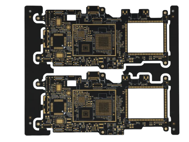
Via protection cannot be added safely after the stackup is frozen. Drill spans, subcomposite thickness, dielectric flow, copper density, press cycles, and later plating all affect whether a hole can be filled and capped.
Q9: How do filled vias interact with sequential lamination?
In a sequential build, some vias are formed, plated, filled, and prepared before later layers or vias are created. The exact order depends on whether the structure uses laser microvias, mechanically drilled blind/buried vias, stacked or staggered transitions, and how many lamination cycles are required.
A stacked microvia places the next interconnect over a previous one, so the underlying fill/cap interface becomes load-bearing and electrically critical. Increasing the number of stacked interfaces can increase registration and reliability risk. A staggered arrangement may use more routing area but avoid placing every interface in one vertical column. The correct choice follows package escape, layer count, capture-pad geometry, reliability class, and fabricator-qualified construction.
The release drawing should show every drill span and lamination stage, not just the final cross-section. Ask for a process-flow review before layout so the design does not depend on an unsupported combination of aspect ratio, dielectric thickness, cap diameter, or stacked depth.
Q10: How does prepreg resin content affect fill and thickness?
Resin content is one input to pressed thickness and copper-pattern encapsulation, but “higher RC fills better” is incomplete. Flow also depends on resin system, glass style, prepreg age and condition, heating rate, pressure, vacuum, copper thickness, retained copper area, feature spacing, panel position, and the supplier’s process window.
Provide layer-by-layer copper density data and the required finished dielectric thickness. The fabricator should return a production construction with prepreg plies, supplier/style, resin content or controlled construction identifier, predicted pressed thickness, and impedance geometry. Verify critical thicknesses by microsection or another agreed method on the first build.
Build a Controlled Material Identity Record
Material selection becomes auditable only when “FR-4,” “low loss,” or a family name is replaced by a controlled construction identity. This is especially important when simulation, impedance, insertion loss, phase, thermal cycling, or qualification depends on the material.
Q11: Why do datasheet Dk and Df differ from the finished board?
Dk and Df values depend on composition, resin content, glass reinforcement, copper treatment, temperature, moisture conditioning, frequency, specimen orientation, and test method. A typical datasheet value is useful for comparison within its stated context; it is not automatically the design value for a specific pressed construction.
Measurement methods excite samples differently and can include different field distributions or conductor effects. Compare Df only under compatible methods, frequencies, conditions, and definitions; do not treat a generic solver Dk as an as-built guarantee.
Use a material identity record:
| Record field | Minimum controlled content |
|---|---|
| Supplier and product family | Exact manufacturer and grade, including slash-sheet or applicable specification |
| Laminate/prepreg construction | Core thickness, prepreg style/plies, resin content or construction code |
| Reinforcement | Glass style, spread/flat-weave designation where applicable, orientation |
| Copper | Foil type, starting/finished thickness, profile or roughness category, bonding treatment |
| Electrical data | Dk/Df value, test method, test frequency, direction, conditioning, source revision |
| Mechanical/thermal data | Tg method, Td, CTE, moisture and other project-critical properties |
| Process data | Lamination and drilling compatibility, desmear/plating route, approved substitutions |
| Design model | Value used in solver, owner, revision, and correlation status |
| As-built evidence | Finished dielectric/copper geometry, coupon result, microsection or loss result |
This record is a stronger control than a private “factory experience number” with no construction, method, or revision attached.
Q12: Can material be selected by data rate or a fixed Df threshold?
No universal rule maps “5 Gb/s,” “25 Gb/s,” or “56 Gb/s” directly to one laminate class. Channel loss depends on signaling method, rise time, Nyquist frequency and harmonics, route length, layer geometry, copper roughness, dielectric loss, vias, connectors, packages, crosstalk, equalization, temperature, and required margin.
Start with the interface channel budget and source/receiver requirements. Model the released stackup, conductor profile, transitions, and interconnects over the required frequency range. A short channel may meet margin on a cost-effective material while a long channel at the same data rate may need lower loss. RF and mmWave circuits may prioritize Dk consistency, phase, conductor surface, and environmental stability differently from high-speed digital channels.
Rogers’ official description is also an important classification correction: RO4350B is a woven-glass-reinforced hydrocarbon/ceramic laminate with electrical performance close to PTFE/woven glass and processing similar to epoxy/glass. It is not a PTFE laminate. That difference affects how a hybrid stackup, drilling route, and bonding system should be discussed.
Select Prepreg, Core, and Glass Construction
Q13: Should critical impedance layers always use core instead of prepreg?
Core is fully cured laminate; prepreg is partially cured bonding material that flows and cures during lamination. Core may offer a convenient supplier-controlled starting thickness, while prepreg enables bonding and copper-pattern encapsulation. However, either can form a controlled-impedance dielectric when the construction and process are characterized.
Do not use generic claims such as “core is always plus or minus five percent and prepreg is always plus or minus ten percent.” Actual tolerances depend on supplier product, nominal thickness, glass/resin construction, press result, copper distribution, and the fabricator’s control plan. Choose core or prepreg around a signal layer by routing/reference needs, lamination architecture, thickness target, resin-fill demand, symmetry, availability, and demonstrated process capability.
For every impedance layer, obtain the as-built dielectric target and tolerance, finished copper geometry, solder-mask model where applicable, and production compensation. The coupon should represent the same structure closely enough to answer the acceptance question.
Q14: How should glass weave be selected?
Woven glass improves mechanical stability but creates local glass-rich and resin-rich regions with different dielectric behavior. A tightly spread or flatter weave can reduce the size of those local windows, but its benefit depends on trace geometry, routing direction, pair spacing, dielectric thickness, glass orientation, and material availability.
Do not specify a glass style only because a blog labels it “high speed.” Ask the laminate supplier and fabricator for the exact construction and reinforcement options that meet thickness, resin, processing, and electrical needs. For dense differential routing, review whether both traces sample similar material regions over the critical length.
Q15: Is routing every differential pair at 10–20 degrees a universal skew fix?
No. Angled routing is one possible averaging strategy, but no single angle is correct for every weave pitch, trace pitch, board orientation, route length, and panel construction. Angling can also consume space, complicate length tuning, and create new coupling or reference-path issues.
Mitigation options include:
- using spread or flatter glass constructions;
- selecting routing position and direction with known glass orientation;
- increasing the statistical averaging of both traces without violating other constraints;
- keeping the pair geometry and reference continuous;
- including package and connector delay in the skew budget;
- using representative coupons or channel measurements where skew risk is material.
The acceptance target should be an interface-derived in-pair skew or channel requirement, not compliance with a routing-angle folklore rule.
Qualify Hybrid Stackups and Surface Finish
Q16: When does a hybrid stackup make sense?
A hybrid construction can place a lower-loss or RF-optimized material only where it earns electrical margin while using a more economical material elsewhere. It is attractive for RF/digital combinations and long high-speed channels, but the savings are real only if the mixed construction is manufacturable and qualified.
Review these items before layout:
| Hybrid-stackup item | Release question |
|---|---|
| Functional layer placement | Which channels require the specialty material, and what modeled margin does it add? |
| Bonding system | Which prepreg or bondply is approved for both surfaces and the selected press cycle? |
| Thermal compatibility | Are in-plane/z-axis expansion and stress acceptable through fabrication, assembly, and use? |
| Drilling and hole preparation | Do smear removal, plasma, chemistry, and plating work across all materials? |
| Copper and surface treatment | Are foil profile and bonding treatment included in the electrical and adhesion model? |
| Registration and dimensional behavior | Can the mixed materials hold the required feature alignment through lamination? |
| Material availability | Are exact grades, thicknesses, and alternates controlled for prototype and volume? |
| Qualification evidence | What coupons, microsections, thermal tests, and channel measurements close the risk? |
“Rogers plus FR-4” is not a complete stackup. State the exact Rogers family, the exact companion laminate/prepreg, constructions, copper, drill spans, bonding route, and qualification plan.
Q17: Must ENIG be avoided above 10 GHz?
No universal frequency cutoff makes ENIG unacceptable. ENIG includes nickel beneath immersion gold on exposed copper, and nickel can add loss or alter behavior in RF structures where current significantly traverses the finished surface. But solder-mask-covered transmission lines do not necessarily carry that finish along their entire length, and system impact depends on geometry, exposed length, launch design, field distribution, and margin.
Choose the finish from solderability, wire-bonding or contact needs, corrosion/shelf-life requirements, pad geometry, assembly process, RF behavior, cost, and supplier control. Where finish loss matters, model or measure representative structures with the intended finish and reference planes. ENEPIG, OSP, immersion silver, immersion tin, and other finishes have different process and reliability tradeoffs; none is a universal high-frequency winner.
Control Impedance, Warpage, and Reliability
Q18: Why do simulated and measured impedance differ?
A field solver calculates the geometry and material model it receives. The PCB contains finished trace width and trapezoid, copper thickness, pressed dielectric thickness, local resin/glass composition, solder mask, copper roughness, and process variation. If the model uses nominal artwork width, generic Dk, or uncured prepreg thickness, agreement can be poor even when fabrication is stable.
Use this correlation loop:
- Release target impedance, tolerance, layer, trace class, reference planes, and coupon intent.
- Receive the fabricator’s proposed production stackup and compensated geometries.
- Simulate with controlled material and finished-geometry assumptions.
- Fabricate a representative coupon with the board.
- Measure by the agreed TDR method and retain waveform, reference plane, calibration, coupon coordinates, and lot/revision.
- Microsection representative structures when geometry correlation is needed.
- Update the controlled model only after identifying whether the difference came from geometry, material assumption, measurement setup, or sampling.
An impedance coupon does not prove every high-speed channel. It verifies the represented transmission structure under the defined method. Long-channel insertion loss, via discontinuities, connectors, and package launches may need separate S-parameter or system evidence.
Q19: How should warpage, solder mask, CAF, and moisture be handled?
These risks interact with stackup and material but need separate acceptance plans.
Warpage: A balanced construction and mirrored copper distribution often help, but perfect symmetry may be impossible when the functional layer map is asymmetric. Model the mechanical intent, balance copper where electrically safe, coordinate panelization and press strategy, and measure bow/twist against the applicable product requirement after the relevant thermal exposure.
Solder mask: LPI solder mask is common for dense boards, but dam capability, registration, thickness over traces, via coverage, color, cure, and final finish compatibility are supplier/process questions. Include mask in outer-layer impedance models when its field interaction matters. For via protection, do not substitute a mask tent or plug for a specified resin-filled-and-capped structure.
CAF: Conductive anodic filament risk depends on electric field, spacing, glass/resin interface, moisture, ionic contamination, drilling damage, material system, and time/temperature. Specify the environment and reliability target, use an appropriate CAF-resistant construction when justified, control hole quality and cleanliness, and qualify the actual spacing/material/process combination.
Moisture: Water uptake can affect insulation, delamination risk, and electrical behavior. PCB storage and bake decisions must follow the material, finish, packaging history, assembly process, and supplier guidance. Do not apply component moisture-sensitivity classifications directly to bare boards without a controlled board-handling specification.
Q20: How do flex and metal-core materials fit this guide?
For flex and rigid-flex, material decisions include adhesiveless versus adhesive-based copper-clad laminate, rolled-annealed versus electrodeposited copper, coverlay/adhesive, bend direction, dynamic or static use, bend radius, copper grain orientation, stiffeners, and transition-zone design. Repeated-flex life is a finished construction and use-condition result, not a promise from “PI” alone. Coordinate the exact build with a flex PCB manufacturing review.
For metal-core PCBs, a headline thermal conductivity value is not enough. Dielectric thickness, thermal resistance, breakdown/withstand requirement, copper area, metal base, interface material, mounting, airflow, and heat-source footprint all contribute. A 1–3 W/m·K dielectric may be adequate in one assembly and inadequate in another; a higher number can still fail if the dielectric is thick or the external heat path is poor. Review the complete thermal and insulation architecture through metal-core PCB engineering.
Diagnose Via-Filling Failure Modes
Via filling should be released with a defect-to-evidence map. Otherwise, “inspect filled vias” may become a visual check that cannot see the critical interface.
| Failure mode | Likely contributors | Why it matters | Evidence or containment |
|---|---|---|---|
| Incomplete fill or internal void | Fill window, trapped gas, aspect ratio, paste condition, poor hole preparation | Weak support, outgassing, inconsistent cap foundation | Representative microsection; process parameters; supplier-specific limits |
| Resin recession or dimple | Cure shrinkage, underfill, planarization, thermal exposure | Paste-volume variation and weak pad support | Surface planarity inspection before/after cap; microsection |
| Protruding fill or crown | Excess fill, cure/planarization control | Component stand-off or print variation | Surface inspection and height/flatness check |
| Thin, porous, or discontinuous cap | Surface preparation, plating distribution, residual depression | Crack/open risk and poor solderable surface | Cap-plating measurement and microsection |
| Cap-to-pad separation | Contamination, adhesion, CTE mismatch, cure state | Intermittent electrical or solder-joint failure | Thermal qualification plus microsection/failure analysis |
| Solder wicking | Open/partially protected via, cap defect, unsuitable land/paste design | Starved SMT joint | Assembly trial, X-ray/sectioning, stencil review |
| Blowhole or outgassing | Entrapped solvent/moisture/air, incomplete cure | Voids, spatter, pad damage during reflow | Cure and storage review; representative reflow trial |
| Barrel or corner crack | Copper/plating geometry, z-axis strain, drilling damage, thermal cycles | Open circuit after assembly or life cycling | Microsection and applicable thermal-stress/cycling plan |
| Stacked-microvia interface separation | Weak cap interface, repeated stacking, process/geometry limits | Latent HDI interconnect failure | Qualified construction, daisy-chain vehicle, cycling and sectioning |
| Material substitution drift | Uncontrolled paste, laminate, glass, copper, or process change | Previously correlated result no longer applies | Approved-source list, change notification, requalification triggers |
Microsection is destructive and sampled, so section location matters. Select representative hole sizes, aspect ratios, panel positions, stacked structures, and thermal-risk regions. X-ray can help locate gross voids or hidden assembly conditions, but it does not replace metallographic evidence for barrel, resin, and cap interfaces.
Qualify Substitute Materials
A datasheet match does not qualify a substitute. Laminate, prepreg, or fill-resin changes can alter pressed geometry, electrical behavior, fabrication response, warpage, cure, planarization, and cap adhesion.
Use a controlled qualification package:
| Qualification element | Required comparison |
|---|---|
| Identity and availability | Manufacturer, grade, construction, plant/source, lifecycle and lead time |
| Electrical properties | Dk/Df under comparable method/frequency/condition; loss/phase model impact |
| Thermal properties | Tg method, Td, CTE, time-to-delamination data where relevant, thermal conductivity |
| Mechanical/process behavior | Thickness, flow, copper adhesion, drill/desmear/plating compatibility, dimensional behavior |
| Reliability | CAF/moisture requirements, plated-hole or microvia cycling, application-specific tests |
| Stackup impact | Finished dielectrics, trace width/spacing, impedance, copper balance, total thickness |
| Prototype evidence | Coupon TDR/loss, microsections, assembly/reflow trial, functional/system tests |
| Change control | Approval owner, affected part numbers, revision, deviation period, requalification trigger |
For high-speed or RF designs, compare the complete channel model, not just Dk and Df. For high-reliability builds, run the required thermal and environmental vehicle. For ordinary products, the qualification can be proportionate, but it still needs a documented owner and release decision.
Plan Cost Without Cutting Evidence
Via filling cost is driven by the number and range of controlled holes, dedicated drill/plating operations, material, cure, planarization, cap plating, sequential laminations, panel utilization, inspection, coupons, and yield. A drawing that mixes requirements or marks unnecessary holes for filling can be more expensive than the resin itself.
Cost-down should follow this order:
- Confirm which holes truly need sealing or a solderable cap.
- Move vias off pads where routing and electrical performance allow.
- Standardize drill spans and feasible hole ranges.
- Reduce sequential-lamination cycles or stacked depth where the package escape permits.
- Use specialty laminate only on layers where the loss or RF budget proves its value.
- Keep inspection representative but capable; do not delete evidence that closes the dominant risk.
- Prequalify realistic material alternates before a supply interruption.
Do not replace Type VII with a mask plug solely to lower price when an SMT joint sits over the feature. Conversely, do not pay for conductive fill where a non-conductive resin and copper barrel meet the released thermal/electrical evidence.
Via Filling and Stackup RFQ Checklist
A useful RFQ lets the manufacturer return a buildable stackup and identify exceptions before quotation becomes a production commitment.
Design files and revision
- Native PCB data if available, synchronized Gerber X2/ODB++/IPC-2581 or other agreed manufacturing data, NC drill files, netlist, fabrication drawing, and readme.
- Unique project, board, assembly, and revision identifiers.
- Board outline, thickness/tolerance, layer count, panel or array requirements, and quantities by prototype/pilot/volume stage.
- Controlled-impedance net classes and the source requirement for each target/tolerance.
Via and hole definition
- Complete drill table with tool size, finished size, plating status, span, tolerance, and quantity.
- Dedicated via-fill layer or attributes identifying every controlled hole.
- IPC-4761 protection type and whether the requirement is one-sided or two-sided where applicable.
- Via-in-pad component locations, pad geometry, cap requirement, final finish, and planarity need.
- Microvia stack/stagger map and sequential-lamination flow.
- Required microsection structures, sampling, acceptance limits, and report format.
Stackup and materials
- Functional layer map with signal/reference/power intent.
- Preferred laminate and prepreg manufacturers/grades, exact constructions, and allowed alternates.
- Required finished copper, total thickness, dielectric targets, copper foil/profile controls, glass-weave needs, and solder mask.
- Dk/Df values used in simulation with method, frequency, and model owner.
- Tg/Td/CTE, CAF, moisture, flammability, thermal, or other application-driven requirements.
- Hybrid-material bonding and process constraints.
Electrical and performance evidence
- Impedance coupon design/ownership, TDR method, calibration/reference plane, report and sampling.
- Insertion-loss, phase, skew, or VNA coupon requirements where impedance alone is insufficient.
- Bare-board electrical test and netlist source.
- Thermal model boundaries and test points for thermal via claims.
- Assembly profile, stencil/paste concerns, X-ray or sectioning plan for via-in-pad joints.
Reliability, compliance, and change control
- Product class, use environment, expected life, assembly/rework cycles, and qualification plan.
- Applicable IPC or customer specifications and explicit precedence.
- Approved material/process list, change-notification requirement, deviation authority, and requalification triggers.
- Required certificate/report package and lot/revision traceability.
Commercial information
- Prototype, pilot, and forecast volume; target dates; approved production region if constrained.
- Material consignment or approved-source rules.
- Requested quote separation for base fabrication, HDI cycles, filling/capping, coupons/reports, NRE, assembly, test, and logistics.
- Packaging, storage, shelf-life, and shipment requirements.
Reference Standards and Responsibility Boundaries
Use the latest contractually applicable edition and define which document takes precedence. Relevant references may include:
- IPC-4761 — Design Guide for Protection of Printed Board Via Structures
- IPC-2221 — Generic Standard on Printed Board Design
- IPC-2226 — Sectional Design Standard for High Density Interconnect Printed Boards
- IPC-4101 — Specification for Base Materials for Rigid and Multilayer Printed Boards
- IPC-4103 — Specification for Base Materials for High Speed/High Frequency Applications
- IPC-6012 — Qualification and Performance Specification for Rigid Printed Boards
- IPC-A-600 — Acceptability of Printed Boards
- IPC-TM-650 — Test Methods Manual
Standards do not allocate every project responsibility automatically:
| Party | Primary responsibility |
|---|---|
| Product/design owner | Define electrical, thermal, mechanical, environmental, life, compliance, and assembly requirements |
| PCB designer/SI-PI engineer | Release stackup intent, constraints, drill spans, via functions, models, and coupon needs |
| Laminate/fill-material supplier | Provide controlled product identity, technical data, storage, processing, and change information |
| PCB fabricator | Propose a manufacturable construction, control the qualified process, disclose exceptions/changes, and provide specified bare-board evidence |
| Assembly provider | Control paste, stencil, placement, reflow, handling, inspection, and assembly evidence |
| Test lab/system owner | Execute product-level channel, thermal, environmental, safety, and compliance validation at defined boundaries |
HILPCB can fabricate and inspect the released PCB/PCBA scope, but a bare-board coupon or microsection cannot certify finished-product signal margin, junction temperature, regulatory compliance, or field life. Those outcomes depend on components, enclosure, cooling, firmware, loads, assembly, and system use.
How HILPCB Supports Stackup Review
For a useful review, send HILPCB the stackup, controlled-net list, via map, material identity, assembly constraints, and evidence plan before layout is locked. The review should return:
- a proposed build sequence and exact drill spans;
- a production stackup with controlled constructions and finished geometries;
- identified via-fill/cap requirements and manufacturability exceptions;
- impedance or other coupon recommendations tied to the actual structures;
- material availability and any proposed alternatives requiring approval;
- a separated quotation showing the cost of HDI cycles, fill/cap operations, inspection, and reports.
Relevant service discussions can begin with HDI PCB manufacturing, multilayer PCB fabrication, or high-speed PCB engineering. When the data package is ready, submit it through the PCB quote request with the checklist above.
Frequently Asked Questions
Why can't via-filling material selection be judged only by whether the hole fills completely?
Complete fill is only one result. The structure must also provide the required planarity, cap-plating integrity, solder behavior, thermal-cycle reliability, compatibility with the laminate and lamination sequence, and evidence at the correct interface.
When must via filling be considered together with stackup design?
Consider it before stackup and layout release whenever the board uses via-in-pad, filled-and-capped vias, stacked microvias, sequential lamination, fine-pitch packages, controlled impedance near filled structures, or a quantified thermal/reliability objective.
Why can't substitute materials be selected from a datasheet alone?
Similar headline Dk, Df, or Tg values do not prove equivalent test methods, constructions, resin flow, drilling, desmear, plating, cap adhesion, warpage, or channel performance. Qualification must compare the released construction and close the relevant electrical, process, assembly, and reliability risks.
At what stage is this via-filling and stackup guide most useful?
It is most valuable during architecture and pre-layout DFM review, when hole type, drill span, laminate construction, copper, assembly geometry, evidence, cost, and material alternates can still be changed without redesigning a finished board.
Conclusion
Reliable via filling begins with a function and ends with evidence. Define why each hole is protected, select the IPC-4761 structure, coordinate it with the lamination sequence, control the fill and laminate identities, and specify how the cap, barrel, stackup, impedance, assembly, and reliability risks will be accepted.
A good via filling material guide therefore produces more than a material name. It produces a build sequence, a controlled stackup, a hole map, an evidence matrix, a qualification path for substitutions, and an RFQ that both design and manufacturing teams can release with confidence.